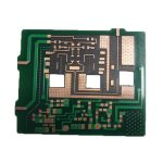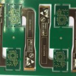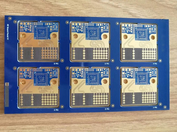
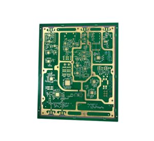
Although different high-frequency PCB products may look almost identical from the outside, their internal materials, manufacturing tolerances, surface conditions, and process controls can be significantly different.
These differences can have a major impact on PCB durability, electrical performance, assembly yield, and long-term reliability. For RF, microwave, and high-speed applications, a small manufacturing variation can sometimes affect impedance, signal loss, insulation performance, or mechanical reliability.
A high-quality high-frequency PCB therefore requires much more than visual inspection. Material selection, copper thickness, cleanliness, dimensional tolerances, solder mask quality, surface finish, via quality, and manufacturing documentation all need to be controlled systematically.
This is particularly important because PCB defects can occur at different stages. A defect may first appear as an assembly problem, but it can also develop into an intermittent electrical failure during actual operation. Such failures can increase repair costs, reduce product reliability, and potentially lead to field returns.
The following 14 requirements provide a practical framework for improving PCB quality control and manufacturing reliability.
1. Maintain Adequate Copper Thickness in Plated Holes
For demanding applications, plated through-hole copper thickness should be controlled according to the applicable IPC class and customer requirements.
A commonly specified minimum finished copper thickness in plated holes is approximately 25 μm for certain reliability-oriented requirements, but the exact requirement depends on the applicable standard, product class, board construction, and customer specification.
Benefits
Adequate plated-hole copper thickness improves:
- Electrical continuity
- Thermal reliability
- Resistance to mechanical stress
- Resistance to Z-axis expansion
- Long-term interconnection reliability
Risks of Insufficient Copper Thickness
If plated-hole copper is too thin, the board may become more susceptible to:
- Hole-wall cracking
- Barrel cracking
- Interlayer connection failure
- Separation or delamination
- Reliability failures under thermal cycling
For high-reliability high-frequency PCB manufacturing, copper thickness should be verified through appropriate process inspection rather than assumed from nominal plating settings.
2. Control PCB Cleanliness Beyond the Minimum Requirement
Cleanliness is an important part of PCB reliability.
During PCB manufacturing and assembly, residues may remain on the board surface if cleaning and process control are inadequate. These residues can include ionic contamination, flux residues, chemicals, dust, and other process-related contaminants.
Benefits
Strict cleanliness control can improve:
- Insulation resistance
- Solder mask reliability
- Surface quality
- Corrosion resistance
- Long-term electrical stability
Risks of Poor Cleanliness
Residual ionic contamination can absorb moisture and contribute to electrochemical migration, corrosion, leakage current, and insulation failure.
For high-frequency and high-impedance circuits, contamination can also create unpredictable electrical behavior.
Therefore, cleanliness requirements should be established according to the application, assembly process, and reliability requirements, with ionic cleanliness testing performed where appropriate.
3. Control Copper-Clad Laminate Thickness and Tolerance
The dielectric structure of a PCB directly affects its electrical characteristics.
For an impedance-controlled high-frequency PCB, variations in dielectric thickness and dielectric constant can change characteristic impedance and signal propagation behavior.
Benefits
Tight material tolerances help provide:
- More consistent impedance
- More predictable signal loss
- Better dimensional stability
- Reduced electrical variation between production lots
- More consistent RF performance
Risks of Excessive Material Variation
If dielectric thickness or material properties vary significantly, the resulting impedance may deviate from the design target.
This can affect:
- Insertion loss
- Return loss
- Signal reflection
- Phase characteristics
- High-speed signal integrity
For this reason, material specifications should be agreed upon before production, especially when specialized high-frequency laminates are used.
4. Control Mechanical Dimensions and Feature Tolerances
The tolerances of board dimensions, holes, slots, cutouts, and other mechanical features should be clearly defined.
Benefits
Good dimensional control improves:
- Component alignment
- Mechanical fit
- Assembly accuracy
- Connector positioning
- Product consistency
Risks of Poor Dimensional Control
Excessive dimensional variation can cause problems such as:
- Misalignment during assembly
- Connector fitting problems
- Fixture interference
- Mounting-hole mismatch
- Mechanical stress during installation
These problems may not become apparent until the PCB reaches final assembly.
For complex RF products, mechanical tolerances should therefore be considered together with electrical and thermal requirements.
5. Use Qualified and Traceable PCB Materials
Material selection is particularly important for high-frequency PCB manufacturing.
Instead of choosing an unfamiliar laminate solely because of its lower cost, manufacturers should use materials with stable and traceable electrical and mechanical specifications.
Important material parameters may include:
- Dielectric constant (Dk)
- Dissipation factor (Df)
- Thermal expansion coefficient
- Glass-transition temperature (Tg)
- Moisture absorption
- Copper adhesion
- Dimensional stability
Benefits
Qualified materials provide more predictable:
- Electrical performance
- Mechanical behavior
- Thermal reliability
- Manufacturing consistency
Risks of Poor Material Selection
Unsuitable materials can contribute to:
- Delamination
- Warpage
- Poor copper adhesion
- Via reliability problems
- Impedance variation
- Excessive dielectric loss
For demanding RF and microwave applications, material selection should always be based on the actual operating frequency and performance requirements.
6. Avoid Unnecessary Soldering or Electrical Repairs
A properly manufactured PCB should not depend on uncontrolled soldering or conductor repairs to meet its intended performance.
Repair may sometimes be technically permitted under a controlled manufacturing procedure, but any repair must be evaluated according to customer requirements and applicable standards.
Benefits
Minimizing unnecessary repairs helps maintain:
- Electrical reliability
- Mechanical consistency
- Long-term durability
- Product traceability
Risks of Improper Repair
Poorly controlled repair can cause:
- Open circuits
- Insufficient conductor adhesion
- Localized mechanical weakness
- Solder-related defects
- Intermittent failures under vibration or thermal cycling
For RF circuits, repairs may also alter local conductor geometry and potentially affect impedance or RF performance.
7. Use a Qualified Solder Mask System
The solder mask protects exposed copper and provides electrical insulation and environmental protection.
Solder mask materials should be selected and qualified according to the applicable PCB requirements and customer specifications.
Where required, materials may need to meet relevant IPC solder-mask requirements and safety certifications.
Benefits
A qualified solder mask can provide:
- Strong adhesion
- Good insulation
- Chemical resistance
- Heat resistance
- Mechanical protection
- Improved corrosion protection
Risks of Poor Solder Mask Quality
Poor-quality or poorly cured solder mask may result in:
- Peeling
- Blistering
- Cracking
- Poor adhesion
- Reduced insulation resistance
- Copper corrosion
Proper surface preparation, coating thickness, exposure, development, and curing are therefore essential parts of PCB quality control.
8. Control the Shelf Life of PCB Surface Finishes
PCB surface finish directly affects solderability, corrosion resistance, storage stability, and assembly reliability.
Common surface finishes include:
- ENIG
- HASL
- Immersion silver
- Immersion tin
- OSP
Each surface finish has different storage and handling requirements.
Benefits
Proper surface-finish control improves:
- Solderability
- Surface reliability
- Corrosion resistance
- Assembly consistency
- Storage performance
Risks of Expired or Improperly Stored Boards
A degraded surface finish can lead to:
- Poor solder wetting
- Oxidation
- Surface contamination
- Interfacial reliability problems
- Assembly defects
Moisture absorption can also contribute to delamination or other reliability problems during reflow.
Therefore, manufacturers should control both the surface-finish process and the storage conditions after production.
9. Control Solder Mask Thickness
Although solder-mask thickness requirements may depend on the application and applicable specification, controlling thickness consistently is important.
Benefits
Appropriate solder-mask thickness helps provide:
- Electrical insulation
- Copper protection
- Mechanical protection
- Better adhesion
- Improved resistance to chemical and environmental exposure
Risks of Insufficient Thickness
An excessively thin solder mask may increase the risk of:
- Poor insulation
- Copper exposure
- Scratching
- Adhesion failure
- Corrosion
On the other hand, excessive solder mask can also interfere with fine-pitch assembly and solder-mask openings.
Therefore, the objective should be controlled and uniform solder-mask thickness, not simply making the coating as thick as possible.
10. Define Appearance and Repair Requirements Clearly
Not every cosmetic imperfection has the same electrical significance, but appearance criteria should be clearly defined for production and inspection.
Typical inspection items include:
- Scratches
- Dents
- Copper exposure
- Solder-mask damage
- Surface contamination
- Burrs
- Delamination
- Improper repairs
Benefits
Clear appearance standards help manufacturers distinguish acceptable cosmetic variation from defects that could affect function or reliability.
Risks of Undefined Requirements
Without clear acceptance criteria, different inspectors may interpret the same defect differently.
This can result in inconsistent quality judgments and potentially allow hidden manufacturing problems to pass inspection.
For this reason, customer drawings, inspection standards, approved samples, and repair criteria should be clearly documented.
11. Apply a Formal Approval Process to Every PCB Purchase Order
Every PCB production order should undergo a controlled engineering and specification review before manufacturing begins.
The review should confirm:
- Gerber or ODB++ data
- Stack-up
- Material
- Copper thickness
- Surface finish
- Impedance requirements
- Hole specifications
- Tolerances
- Solder mask
- Silkscreen
- Testing requirements
- Special process requirements
Benefits
A formal approval process ensures that design and manufacturing requirements are understood before production.
Risks of Inadequate Review
If specifications are not carefully reviewed, deviations may only be discovered during assembly or final-product testing.
At that stage, correcting the problem can result in significant cost and schedule delays.
12. Specify Peelable Mask Material and Process Requirements
When peelable solder mask or temporary protective material is required, its specification should be clearly defined.
Important factors include:
- Material type
- Manufacturer
- Model
- Application method
- Curing conditions
- Peelability
- Compatibility with surface finish
- Compatibility with assembly temperatures
Benefits
Qualified peelable materials can protect selected PCB areas during manufacturing and assembly without leaving excessive residue.
Risks of Poor-Quality Material
Unqualified materials may:
- Bubble
- Melt
- Crack
- Become difficult to remove
- Leave residues
- Affect solderability
Therefore, peelable materials should be validated before production rather than selected solely on price.
13. Control Via Filling and Plugging Quality
For boards requiring plugged or filled vias, the filling depth and quality should be clearly specified.
This is especially important for high-frequency PCB designs using via-in-pad structures, fine-pitch components, or advanced HDI technology.
Benefits
Proper via filling can reduce:
- Solder wicking
- Solder-ball formation
- Voids
- Surface contamination
- Assembly defects
It can also improve the reliability of fine-pitch component attachment.
Risks of Inadequate Via Filling
Poorly filled holes may trap chemicals or moisture and can create soldering problems.
During assembly, uncontrolled solder flow or trapped material may contribute to solder balls, voids, or electrical shorts.
For via-in-pad applications, filled and appropriately finished vias should be evaluated according to the component land pattern and assembly process.
14. Clearly Identify and Isolate Defective PCB Units
When a production panel contains defective units, the rejected units must be clearly identified and controlled.
Benefits
Effective defective-unit management prevents known failures from entering assembly.
It also helps:
- Reduce component waste
- Prevent unnecessary assembly costs
- Improve production traceability
- Protect final-product quality
Risks of Poor X-Out Management
If defective units are not clearly marked or physically separated according to the agreed production procedure, they may accidentally enter the assembly line.
This can result in wasted components, additional labor, rework, and unnecessary troubleshooting.
For production panels containing multiple PCB units, the supplier and assembler should agree in advance on the acceptable panelization and defective-unit identification method.
Additional Quality Controls for High-Frequency PCBs
The 14 requirements above provide a strong foundation, but advanced high-frequency PCB manufacturing requires additional controls because RF performance can be sensitive to small physical variations.
Impedance Control
Controlled-impedance traces should be designed and manufactured according to the agreed stack-up.
The final impedance is influenced by:
- Trace width
- Copper thickness
- Dielectric thickness
- Dk
- Reference-plane distance
- Trace geometry
- Copper roughness
Impedance testing should be performed when required by the design.
Registration Accuracy
Multilayer and HDI boards require accurate layer registration.
Poor registration can change trace width, spacing, via capture-pad geometry, and impedance.
Copper Surface Roughness
At higher frequencies, conductor surface roughness can increase conductor loss because of the skin effect.
Therefore, high-frequency designs may require controlled copper roughness and appropriate copper foil specifications.
Thermal Reliability
High-frequency PCBs used in automotive, communication, aerospace, and industrial systems may experience repeated temperature changes.
Material selection and plated-hole construction should therefore be evaluated for thermal expansion and thermal cycling reliability.
Kingda’s Approach to High-Frequency PCB Quality
Kingda emphasizes process control throughout the PCB manufacturing cycle, from engineering review and material selection to fabrication, inspection, and final testing.
For demanding high-frequency PCB manufacturing, quality control can include:
- Material verification
- Stack-up review
- Impedance control
- Copper-thickness inspection
- Hole-quality inspection
- Layer-registration control
- Surface-finish inspection
- Solder-mask inspection
- Electrical testing
- Dimensional inspection
- Final visual inspection
The objective is not simply to produce a PCB that passes a basic electrical test, but to ensure that the board maintains stable performance throughout assembly and its expected service life.
Conclusion
A high-frequency PCB may look similar to a conventional circuit board, but its internal construction and manufacturing requirements can be considerably more demanding.
From plated-hole copper thickness and material selection to cleanliness, dimensional tolerance, solder mask, surface finish, via filling, and defective-unit control, every process can influence final PCB reliability.
For RF, microwave, automotive, communication, and high-speed applications, quality should therefore be treated as a complete manufacturing system rather than a final inspection step.
By combining qualified materials, controlled manufacturing processes, clear engineering specifications, and comprehensive PCB quality control, manufacturers such as Kingda can help customers achieve stable electrical performance, reliable assembly, and long-term product durability.