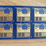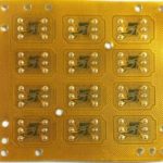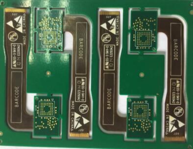
Compared with conventional circuit boards, an advanced PCB typically features more layers, denser traces and vias, larger panel or unit sizes, thinner dielectric layers, and more demanding electrical and mechanical requirements.
As electronic products continue to become smaller, faster, and more highly integrated, PCB designs are becoming increasingly complex. High-Tg, high-speed, high-frequency, thick-copper, HDI, and rigid-flex constructions are now widely used in communication equipment, automotive electronics, aerospace systems, medical devices, and other advanced applications.
These complex structures place greater demands on advanced PCB manufacturing, particularly in layer alignment, inner-layer fabrication, lamination, material selection, interlayer interconnection, and long-term reliability.
Rigid-flex technology introduces another level of complexity by combining rigid and flexible PCB structures within a single board. This requires carefully coordinated material selection and manufacturing processes to ensure both electrical performance and mechanical durability.
Major Challenges in Advanced PCB Manufacturing
1. Difficulties in PCB Layer Alignment
As the layer count and circuit density of an advanced PCB increase, layer-to-layer registration becomes increasingly important.
Multilayer PCB fabrication involves repeated imaging, lamination, drilling, plating, and alignment processes. Dimensional changes can occur because of:
- Temperature and humidity variations
- Resin shrinkage during curing
- Thermal expansion
- Copper distribution
- Core-material characteristics
- Lamination pressure and temperature
- Different material expansion coefficients
These factors can accumulate throughout the manufacturing process and make precise PCB layer alignment more difficult.
Poor registration can result in:
- Misaligned pads
- Reduced annular rings
- Via-to-pad offset
- Trace-width variation
- Insufficient spacing
- Open or short circuits
- Reduced assembly reliability
For high-density multilayer boards, manufacturers therefore need accurate registration systems, stable process conditions, appropriate compensation models, and strict process monitoring.
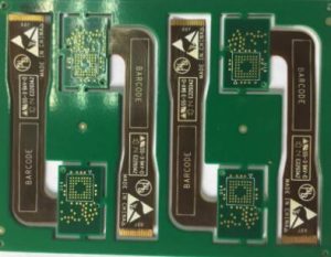
2. Difficulties in Inner-Layer Circuit Fabrication
The inner layers of an advanced PCB can be particularly difficult to manufacture when the design combines fine traces, narrow spacing, high-speed signals, high-frequency materials, thick copper, and thin dielectric layers.
Fine-Line Circuit Requirements
Smaller trace widths and spaces reduce the manufacturing process window.
Small variations during imaging or etching can result in:
- Open circuits
- Short circuits
- Excessive etching
- Insufficient etching
- Trace-width variation
- Reduced yield
For impedance-controlled circuits, trace geometry must remain consistent because trace width, copper thickness, dielectric thickness, and reference-plane distance directly influence characteristic impedance.
Inner-Layer Inspection
As circuit density increases, detecting defects on internal layers becomes more challenging.
Automated optical inspection (AOI) is therefore important for identifying defects before lamination. Proper AOI coverage and inspection criteria help prevent defective inner-layer cores from entering subsequent manufacturing stages.
Thin Core Handling
Thin inner-layer cores can be more susceptible to:
- Wrinkling
- Scratching
- Dimensional deformation
- Handling damage
These problems can affect exposure, imaging, etching, and registration.
Careful material handling and process control are therefore essential for advanced PCB manufacturing.
Large-Format PCB Considerations
Many advanced system boards use relatively large unit sizes.
When a defect occurs on a large board, the material and processing costs associated with scrap can be significantly higher than those of a small conventional PCB.
This makes early defect detection and process capability control particularly important.
3. Lamination Challenges
Lamination is one of the most critical processes in multilayer advanced PCB manufacturing.
A multilayer PCB may contain multiple cores, copper foils, prepregs, and specialized dielectric materials. During lamination, these materials must form a stable and uniform structure.
Potential defects include:
- Layer shifting
- Delamination
- Resin voids
- Air entrapment
- Resin starvation
- Excessive resin flow
- Uneven dielectric thickness
- Interlayer bonding failure
Material Selection and Lamination Design
The lamination structure should be developed based on the characteristics of the selected materials.
Important parameters include:
- Resin content
- Resin flow
- Dielectric thickness
- Glass style
- Curing behavior
- Thermal expansion
- Pressing temperature
- Pressing pressure
- Heating and cooling rates
For mixed-material constructions, these factors become even more important.
Thermal and Mechanical Reliability
Multilayer boards experience dimensional changes during heating and cooling. If the different materials have significantly different coefficients of thermal expansion (CTE), mechanical stress may accumulate at interfaces and plated through-holes.
This can eventually lead to:
- Delamination
- Barrel cracking
- Interlayer separation
- Via reliability failures
Therefore, lamination design must be evaluated together with the expected operating temperature range and reliability requirements.
Rigid-Flex PCB: A Key Advanced PCB Technology
A rigid-flex PCB combines rigid PCB sections with flexible circuit sections in a single integrated structure.
This technology provides the mechanical stability of rigid boards while allowing selected areas to bend or fold.
Rigid-flex technology is increasingly used in:
- Consumer electronics
- Medical equipment
- Automotive electronics
- Aerospace systems
- Industrial equipment
- Cameras
- Wearable devices
- Compact communication equipment
Instead of connecting separate rigid and flexible boards with conventional connectors, a rigid-flex structure can integrate electrical connections directly into one PCB assembly.
This can reduce connector count, save space, improve mechanical integration, and potentially increase system reliability.
Key Rigid-Flex PCB Technologies
1. Material Matching Technology
Material selection is one of the most important aspects of rigid-flex PCB manufacturing.
A rigid-flex board may combine:
- Flexible polyimide substrates
- Rigid FR-4 cores
- Bonding films
- Flexible coverlay
- Prepreg
- Copper foils
- Adhesive systems
These materials have different mechanical and thermal characteristics.
The material combination must therefore be selected according to:
- Bend requirements
- Layer structure
- Operating temperature
- Electrical requirements
- Assembly process
- Mechanical stress
- Expected service life
Incorrect material matching can lead to delamination, cracking, excessive flex stress, or dimensional instability.
2. Multi-Material Layer Alignment
Rigid-flex structures often contain several material systems within the same cross-section.
Achieving accurate PCB layer alignment is therefore more difficult than with a conventional rigid multilayer PCB.
Manufacturers need to control:
- Material expansion and contraction
- Layer registration
- Lamination structure
- Flexible-to-rigid transition geometry
- Coverlay alignment
- Bonding-film thickness
- Pressing parameters
Process development may require multiple engineering trials to establish suitable lamination and registration parameters.
The objective is to achieve both accurate alignment and reliable bonding between rigid and flexible sections.
3. Multilayer Interconnection Technology
A rigid-flex PCB may contain complex interconnections, including:
- Through vias
- Blind vias
- Buried vias
- Microvias
- HDI structures
Different sections of the board may require different drilling and metallization strategies.
For example, rigid sections may use conventional mechanical drilling, while high-density areas may require laser-drilled microvias.
Hole Metallization
Reliable interlayer connection requires stable copper deposition throughout the via structure.
Important process controls include:
- Hole-wall cleanliness
- Surface activation
- Electroless copper
- Electrolytic copper plating
- Copper thickness
- Via filling where required
- Thermal-cycle reliability
The interface between the plated copper and dielectric material must maintain sufficient adhesion throughout the expected operating conditions.
4. Flexible Area Protection
Protecting the flexible region during rigid-flex PCB manufacturing is one of the most important process challenges.
Flexible sections can be more vulnerable to mechanical damage and chemical exposure than rigid PCB areas.
Potential problems include:
- Scratches
- Creases
- Excessive bending
- Chemical attack
- Coverlay damage
- Copper cracking
- Delamination
- Insulation damage
Manufacturers must therefore develop appropriate handling and protection procedures throughout drilling, plating, imaging, etching, solder mask or coverlay processing, routing, and final assembly.
Rigid-Flex PCB Bending Reliability
The flexible section must be designed according to the intended bending mode.
Important design factors include:
- Bend radius
- Number of bending cycles
- Dynamic or static flexing
- Copper thickness
- Copper type
- Trace geometry
- Coverlay structure
- Neutral-axis location
- Stiffener design
For dynamic applications, the flex region must be designed to withstand repeated mechanical movement without copper fatigue or dielectric cracking.
A bend radius that is suitable for static folding may not be suitable for repeated dynamic flexing.
Therefore, mechanical reliability requirements should be defined before finalizing the flexible-region stack-up.
Rigid-Flex Transition Design
The transition between the rigid and flexible sections is a critical area because mechanical stress can concentrate around this region.
Good design practices include:
- Avoid abrupt trace transitions.
- Avoid unnecessary copper concentration changes.
- Use appropriate fillets where applicable.
- Maintain adequate coverlay overlap.
- Avoid placing vias too close to high-flex areas.
- Control the transition geometry.
- Provide appropriate stiffening where required.
The transition zone should be evaluated for both electrical continuity and mechanical stress.
Electrical Performance of Rigid-Flex PCBs
Although rigid-flex boards are often selected for mechanical integration, their electrical performance must also be considered.
For high-speed or RF rigid-flex applications, designers should control:
- Characteristic impedance
- Differential-pair geometry
- Dielectric thickness
- Copper thickness
- Signal-return paths
- Ground-plane continuity
- Via transitions
- Material Dk and Df
The flexible and rigid portions may use different dielectric structures, so impedance can change if the transition is not carefully designed.
For this reason, impedance-controlled rigid-flex designs require close cooperation between PCB design and manufacturing engineering.
How to Improve Advanced PCB Reliability
Reliable advanced PCB production requires process control across the entire manufacturing chain.
Recommended practices include:
- Select materials according to electrical, thermal, and mechanical requirements.
- Establish the PCB stack-up before manufacturing.
- Analyze material expansion and shrinkage.
- Control layer registration.
- Optimize inner-layer imaging and etching.
- Inspect inner-layer circuits before lamination.
- Develop an appropriate lamination profile.
- Control dielectric thickness.
- Optimize drilling and via metallization.
- Protect flexible areas during manufacturing.
- Perform electrical testing and dimensional inspection.
- Validate reliability through appropriate thermal and mechanical testing.
For high-density boards, design-for-manufacturing (DFM) should be performed before production to identify potential issues with trace spacing, via structures, layer registration, material selection, and manufacturing tolerances.
Common Defects in Advanced and Rigid-Flex PCBs
Understanding common defects helps manufacturers establish preventive controls.
Delamination
Delamination occurs when interfaces between materials lose adhesion.
It can result from:
- Poor material compatibility
- Incorrect lamination parameters
- Moisture
- Excessive thermal stress
- Contamination
Via and Barrel Cracking
Repeated thermal expansion and contraction can place stress on plated holes and vias.
Appropriate copper thickness, material selection, drilling quality, and thermal-reliability testing can help reduce the risk.
Registration Errors
Layer misalignment can reduce annular rings and create clearance problems.
This is especially critical for HDI and rigid-flex structures.
Flexible-Circuit Copper Cracking
Excessive bending or an inappropriate bend radius can cause copper fatigue.
The flexible region should therefore be designed and tested according to its actual mechanical requirements.
Kingda’s Advanced PCB Manufacturing Support
Kingda supports advanced PCB projects requiring high layer counts, fine-line structures, controlled impedance, complex via technologies, and rigid-flex construction.
For demanding rigid-flex PCB manufacturing, the manufacturing process should integrate material evaluation, stack-up engineering, registration control, lamination optimization, drilling, plating, flexible-area protection, and final inspection.
Kingda’s approach focuses on combining design-for-manufacturing analysis with controlled production processes to improve yield, consistency, and PCB reliability.
Conclusion
The complexity of modern electronic products continues to push PCB technology toward higher density, thinner dielectric structures, more layers, finer traces, and more sophisticated interconnection technologies.
These requirements make advanced PCB manufacturing increasingly challenging. Layer alignment, inner-layer fabrication, lamination, material compatibility, drilling, plating, and reliability testing must all be carefully controlled.
At the same time, rigid-flex PCB technology provides an effective solution for products that require both mechanical flexibility and rigid structural support. However, combining different materials and manufacturing processes introduces additional challenges in material matching, registration, lamination, interconnection, and flexible-area protection.
By integrating appropriate material selection, precise manufacturing processes, DFM analysis, and comprehensive quality control, manufacturers can produce advanced multilayer and rigid-flex boards with stable electrical performance, strong mechanical reliability, and long-term durability.