High-Speed PCB Basics: When Signals Stop Being Simple
The phrase high-speed is often used as a synonym for high frequency, and that is the first thing a beginner has to unlearn. A bus running at a modest clock rate can behave as a high-speed channel if its edges are fast enough, and a signal at several hundred megahertz can be perfectly well behaved if it changes slowly. What matters is how the signal behaves in time, not how often it repeats.
The Rise Time Test
The useful criterion compares the signal rise time with the time it takes to travel along the trace. When the propagation delay of the interconnect becomes a significant fraction of the rise time, the trace has to be treated as a transmission line. A common rule of thumb is that the interconnect length matters once it exceeds about one sixth of the electrical wavelength of the highest significant frequency component.
That is why a nominally slow interface can appear on the list of high-speed problems. Its clock may be low, but its driver edges may be very fast, and it is the edge that decides whether reflections and crosstalk will be visible. Checking the rise time rather than the clock frequency is the habit that prevents surprises.
Impedance Control
Once the trace is a transmission line, its characteristic impedance governs how energy moves along it. Most single-ended interfaces target 50 ohms and most differential links target 90 or 100 ohms, and the tolerance is usually plus or minus ten percent.
Impedance is set by the trace width, the dielectric constant and the distance to the reference plane. That means microstrip and stripline geometry has to be calculated against the actual stackup rather than chosen from habit, and the calculation repeated for each layer, because the same width gives a different impedance on a different dielectric thickness.
Differential Pairs
A differential pair carries information in the difference between two conductors rather than in their absolute voltage, which makes it resistant to common-mode noise and gives it a predictable return path. The price is that the pair has to be routed as a pair: consistent spacing, matched length, and no interruption to the reference plane beneath.
Practical rules follow from that. Keep the two traces the same length, avoid routing one of them through a via while the other stays on the layer, and do not let a third signal share the gap between them. The routing conventions that keep a differential pair intact are worth learning early, because retrofitting them into a finished layout is expensive.
Loss and Material Selection
Insertion loss has two components. Conductor loss depends on copper surface roughness and trace geometry and rises with the square root of frequency. Dielectric loss depends on the dissipation factor of the laminate and rises linearly with frequency.
Material choice therefore follows frequency. Standard FR-4 has a dielectric constant around 4.5 and a dissipation factor between 0.02 and 0.035, which is acceptable at moderate rates on short channels. Improved FR-4 grades bring the dissipation factor down to roughly 0.006 to 0.01 and shift the dielectric constant to about 3.8 to 4.2. Ceramic-filled laminates reach a dissipation factor near 0.004, and the lowest-loss materials at the top of the range approach 0.0025 with a dielectric constant near 3.2.
Stackup Symmetry and Return Paths
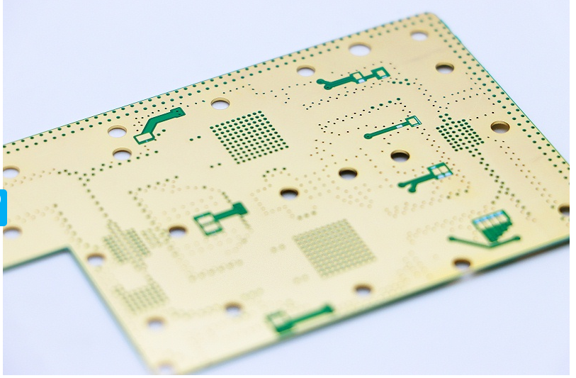
A symmetric stackup, where the layers are arranged evenly around the centre, keeps the panel flat through lamination and keeps the impedance of corresponding layers consistent. An asymmetric stack warps, and on a high-speed board warpage means the dielectric thickness varies across the panel and the impedance varies with it.
Equally important is the return path. Every signal current returns to its source through the reference plane beneath it, and that plane must be continuous for the whole length of the trace. A plane split forces the return current into a detour, which enlarges the loop area, radiates and couples into neighbouring traces. The routing practices that keep this under control are set out in the guidance on high-frequency traces and data buses.
Termination and Reflections
A reflection occurs wherever the impedance changes: at the end of a trace that is not terminated, at a connector, at a via, and at the boundary between two routing layers. Terminating the line at the driver or the receiver absorbs the energy that would otherwise bounce, and choosing the right scheme depends on the topology.
Series termination suits a single point-to-point link and is cheap and quiet. Parallel or Thevenin termination handles multi-drop buses better but consumes static current. Whatever the scheme, the value has to be matched to the actual trace impedance, which is another reason the stackup has to be fixed before the schematic is finalised.
Via Effects and Backdrilling
A via is an impedance discontinuity, and it is also a stub. The portion of the barrel below the layer where the signal leaves the via behaves as an open-ended transmission line, and it resonates at a frequency determined by its physical length. On a thick board at a high data rate, that resonance can fall inside the band the interface is using.
Backdrilling removes the unused portion of the barrel after plating, which removes most of the stub and restores the transition. Blind and buried vias achieve the same result by not passing through the whole board. The choice is a cost question: backdrilling is a separate operation on every hole concerned, while blind and buried vias require sequential lamination.
How to Begin
Start with the stackup and the impedance targets, and work outward from the fastest interface rather than from the board outline. Learn to read an eye diagram and an insertion loss curve, since those two measurements tell you whether a channel has margin or is barely working.
Then practise on a real design with a modest channel: a memory bus or a USB link is a good first project because the rules are documented and the result is measurable. Simulating a simple channel before building it is the fastest way to develop the intuition that a high-speed PCB is mostly about controlled geometry and continuous return paths.
Power Integrity Is Half the Problem
A fast interface only works if the supply feeding it is stable. Load transients on a modern device change in nanoseconds, which is faster than any regulator can respond, so the voltage seen at the die is set by the impedance of the decoupling network and the plane structure across a wide frequency range.
Designing that network means working from a target impedance rather than from a capacitor count, placing the smallest capacitors closest to the pins, and keeping the plane pair that supplies them close together. On a high-speed board, power integrity and signal integrity are the same problem examined from two directions.
FAQ
Is 50 MHz the threshold for high-speed design? It is a rough marker rather than a rule. The reliable test is comparing the rise time with the propagation delay; a slow clock with fast edges can need more care than a fast clock with soft edges.
Do I need a low-loss laminate for a gigabit link? Not always. On a short channel, improved FR-4 with a dissipation factor around 0.008 is often sufficient, and the loss budget calculation will show whether a more expensive material is needed.
How important is via design at these rates? Very. Vias are usually the largest single source of impedance discontinuity on a board, and stub removal through backdrilling or blind vias is often the difference between a link with margin and one that fails intermittently.