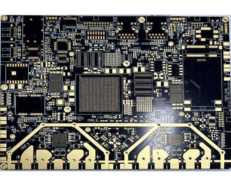
Twelve-Layer PCB: Stackup, Fabrication and Design Practice
Twelve layers is the point where a board stops being a routing problem and becomes an architecture problem. Below that count a designer can usually add a layer to solve a difficulty; at twelve, every layer has to be assigned a purpose and the sequence in which the layers are built has to be planned before any routing begins.
What Twelve Layers Buy You
The first benefit is routing capacity with controlled references. Four to six inner signal layers can each be paired with an adjacent plane, so the return path is continuous for every high-speed net without compromising the other layers. On an eight-layer board that pairing is possible but strained.
The second benefit is power distribution. Independent ground and power planes can serve separate supply domains, which reduces the impedance of the distribution network and keeps switching noise from one domain out of another. The third is shielding: placing sensitive signals between planes reduces both emissions and susceptibility, which matters on a board that carries several fast interfaces at once.
Stackup Planning
The stackup should be drawn before the layout, with each layer labelled by function and each dielectric thickness chosen to hit an impedance target. stackup planning also determines whether the board can be drilled economically, because the distance between a signal layer and its reference is what sets the drill depth for any blind via.
Symmetry is a hard requirement. Twelve layers built as two bonded sub-stacks of six will warp if the copper distribution is uneven, and warping changes dielectric thickness and therefore impedance. Balancing copper across the stack, and keeping the arrangement of the two halves as similar as the design allows, is what keeps the finished board flat and the impedance consistent.

The Fabrication Sequence
The build proceeds in stages. Inner layer cores are imaged and etched, inspected optically, then laminated in pairs with prepreg under heat and pressure. Holes are drilled into the resulting sub-assemblies, plated, and filled where the design requires a filled or capped via, and the surface is planarised before the next lamination.
The sub-assemblies are then bonded together, outer layers are imaged and etched, and the final plated through-holes are drilled and plated. Surface finish, solder mask and legend follow, then profiling to the finished outline. Each lamination cycle adds drilling, plating, planarisation and inspection, which is why the cost of a blind and buried vias structure is felt across the whole board rather than only at the vias.
Materials
Standard FR-4 covers the majority of twelve-layer designs, and high glass transition grades are used where the assembly temperature or the operating environment demands better dimensional stability. High-speed signals push towards laminates with a lower dissipation factor, and radio-frequency sections may need a dedicated low-loss material in a hybrid stackup.
Copper weight is usually one or two ounces, with heavier copper reserved for power layers. Where a hybrid stackup is used, the prepreg that bonds the two materials has to be compatible with both, and the coefficient of expansion of the pair has to be close enough that the lamination does not build in stress that shows up as warpage or delamination later.

Layer Registration
Registration is the tolerance that defines the design rules for a board of this complexity. Every lamination cycle adds a contribution to the accumulated misalignment between layers, and the capture pad at each via has to accommodate the sum of those contributions. That is why pad sizes on inner layers of a twelve-layer board are larger than the trace widths might suggest.
The design response is to limit the number of cycles where possible, keep the site of any critical connection on an early stage of the build, and set the capture pad using the fabricator capability rather than a generic rule. layer registration problems show up as intermittent connections rather than as open circuits, which makes them expensive to diagnose after assembly.
Design Practice
Route the fastest nets first on the layers closest to a plane, and keep each of them on one layer for its whole length where the design allows. Where a net must change layers, place a return via beside the signal via and adjust the trace width for the new dielectric thickness.
Keep the planes intact under every critical signal and place the decoupling capacitors at the pins they serve. On a twelve-layer board the temptation is to use the spare capacity for convenience routing that crosses plane boundaries; that practice is what turns a well-planned stackup into a noisy board.
Thermal Considerations
A dense stack has more copper generating heat and more dielectric insulating it. Thermal via arrays under power devices, connected to internal copper and to a copper area on the opposite side, provide the path out. Where the dissipation is high, the board may also need a spreader or a defined interface to the enclosure.
Copper balancing serves the thermal design as well as the mechanical one, because an unbalanced stack has hot and cool regions that follow the copper distribution. The general routing principles involved are set out in the guidance on multilayer design rules.
Test and Verification
Electrical test covers continuity and isolation, and on a board with several thousand nets a fixture-based test is usually the only method with an acceptable cycle time. X-ray inspection verifies hidden joints and inner layer connections, and impedance coupons fabricated on the same panel confirm that the produced geometry matches the design targets.
Cross sections from a coupon are the evidence for the things no electrical test can see: plating thickness in the barrels, fill quality in capped vias and the actual dielectric thicknesses at each interface. On a twelve-layer build, that evidence is what makes the first article approval meaningful.
When the Layer Count Is Justified
The honest test is whether the design needs the layers or merely wants them. If the routing fits on fewer layers with continuous returns and adequate power distribution, adding layers raises cost, extends lead time and adds yield risk without changing the outcome.
When the interfaces, the supply domains and the shielding requirements together exceed what a simpler stack can provide, twelve layers becomes the economical answer rather than an extravagant one, because the alternative is a design that cannot be built reliably at any layer count.
Keeping Impedance Control Consistent
Every impedance-controlled net on a twelve-layer PCB has to be calculated against the dielectric thickness of the layer it actually travels on. Because a stack of this size usually contains several different dielectric thicknesses, the same target impedance can require noticeably different trace widths from one layer to the next.
The practical way to manage that is to limit the number of layers that carry impedance-controlled nets and to define a small set of trace widths that covers every case. Where a controlled net has to change layers, the width is adjusted at the transition so that the impedance stays inside tolerance on both sides of the via.
FAQ
What is the minimum order quantity for a twelve-layer board? Many fabricators accept small prototype quantities, so a development build is practical. The unit price is dominated by the fixed setup and lamination work rather than by the number of panels.
Can impedance be controlled on every layer? It can, but each layer needs its own calculation because the dielectric thicknesses differ. Coupons are normally placed on several layers so that the produced geometry can be verified across the stack.
How long does fabrication take? A prototype run is usually measured in one to two weeks and a production build in two to four, depending on the number of lamination cycles and the material lead time.