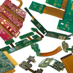
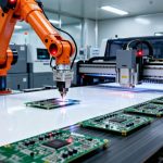
As electronic systems become faster, denser, and more interconnected, controlling signal integrity, power integrity, electromagnetic interference (EMI), and thermal performance has become increasingly important. Modern computing platforms, telecommunications equipment, AI infrastructure, automotive electronics, 5G systems, medical devices, industrial controls, and IoT products all depend on reliable high-speed data transmission.
At the center of these systems are High-Speed PCBs, which are designed to preserve signal quality as electrical signals travel across increasingly fast interfaces.
Unlike conventional PCB designs, high-speed PCB design requires careful consideration of transmission-line behavior, impedance, return paths, crosstalk, stack-up, dielectric properties, routing geometry, and power distribution.
This article explains what a High-Speed PCB is, how it differs from a standard PCB, the major design challenges, key applications, emerging trends, and how Kingda supports high-speed PCB manufacturing and assembly.
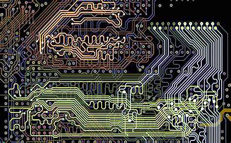
What Are High-Speed PCBs?
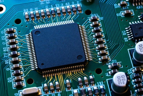
A High-Speed PCB is a printed circuit board designed to maintain reliable signal transmission when the electrical behavior of an interconnect can no longer be treated as a simple lumped circuit.
It is not technically accurate to classify every high-speed PCB using a fixed frequency threshold such as 50 MHz. Whether a design requires high-speed PCB techniques depends on factors such as signal rise time, edge rate, trace length, propagation delay, interface technology, operating frequency, and PCB geometry.
In practical engineering, even a relatively low-frequency digital signal can exhibit transmission-line behavior when its edge rate is sufficiently fast relative to the interconnect length.
High-speed PCB design therefore focuses on controlling the complete electrical path, including:
- Controlled impedance
- Signal propagation
- Return-current paths
- Crosstalk
- Reflections
- Power integrity
- Ground integrity
- EMI/EMC
- Thermal performance
Common high-speed interfaces include PCIe, USB, DDR memory, Ethernet, SerDes, high-speed ADC/DAC connections, and other high-data-rate digital or RF systems.
High-Speed PCB vs. Standard PCB
The main difference between a High-Speed PCB and a conventional PCB is not simply the clock frequency. The difference lies in how carefully electrical interconnect behavior must be controlled.
| No. | High-Speed PCB | Standard PCB |
|---|---|---|
| 1 | Fast signal edge rates make transmission-line effects important | Slower edges may allow simpler interconnect analysis |
| 2 | Signal integrity is a major design requirement | Signal integrity requirements are often less demanding |
| 3 | Precise impedance control is commonly required | Tight impedance control may not always be necessary |
| 4 | Reflections and crosstalk must be actively managed | These effects may be less significant |
| 5 | Stack-up and return paths strongly affect performance | Stack-up is often simpler |
| 6 | Material electrical properties can be critical | Standard materials may be sufficient |
| 7 | Simulation and verification are commonly used | Simulation requirements may be lower |
| 8 | Manufacturing tolerances can directly affect electrical performance | Standard fabrication tolerances may be adequate |
| 9 | Higher engineering and manufacturing complexity | Simpler production requirements |
| 10 | Usually higher overall development and manufacturing cost | Generally more economical |
A conventional PCB remains the more cost-effective choice when signal speeds and electrical requirements do not justify advanced high-speed design techniques.
For demanding interfaces, however, treating a high-speed design like a conventional PCB can lead to signal degradation, excessive EMI, unstable operation, or failure to meet system-level performance targets.
Key Challenges in High-Speed PCB Design
1. Signal Integrity
Signal integrity (SI) is one of the most important concerns in high-speed PCB design.
As signal edge rates increase, PCB traces behave more like transmission lines. Problems such as reflections, ringing, attenuation, crosstalk, and impedance discontinuities can distort the signal.
Typical causes include:
- Incorrect trace impedance
- Long interconnects
- Poor return paths
- Connector discontinuities
- Via transitions
- Inappropriate layer changes
- Excessive stubs
- Improper termination
How to Improve Signal Integrity
Engineers can improve high-speed signal integrity by:
- Maintaining controlled impedance
- Keeping high-speed traces short where practical
- Providing continuous reference planes
- Minimizing unnecessary vias
- Avoiding abrupt geometry changes
- Managing differential-pair spacing
- Reducing stubs
- Using appropriate termination techniques
- Performing SI simulation during design
Modern ECAD tools can simulate and analyze high-speed interconnects before fabrication, helping engineers identify potential problems early.
2. Impedance Control
Controlled impedance PCB design is fundamental for many high-speed interfaces.
Trace impedance depends on several factors, including:
- Trace width
- Copper thickness
- Dielectric thickness
- Dielectric constant
- Distance to reference plane
- PCB stack-up
- Copper roughness
A mismatch between the source, PCB interconnect, and receiver can generate reflections that reduce signal quality.
For this reason, impedance requirements should be established before PCB fabrication.
The manufacturer needs to understand:
- Target impedance
- Layer assignment
- Trace width
- Dielectric structure
- Copper thickness
- Required tolerance
- Test method
Kingda provides controlled-impedance PCB manufacturing and engineering support, including PCB design review and manufacturing optimization for high-speed applications. Its published capabilities also include high-speed and high-frequency PCB manufacturing and assembly. (GOPCBA)
3. Crosstalk
Crosstalk occurs when electromagnetic energy from one signal path interferes with a neighboring signal.
It becomes more problematic when:
- Traces run parallel for long distances
- Spacing is too small
- Signal transitions are fast
- Return paths are poorly controlled
- Routing density is high
Designers can reduce crosstalk by:
- Increasing spacing
- Reducing parallel routing length
- Using appropriate reference planes
- Controlling differential-pair geometry
- Separating sensitive and noisy signals
- Optimizing layer transitions
4. Electromagnetic Interference
High-speed switching can produce strong electromagnetic fields. Poorly designed current loops, discontinuous ground structures, impedance discontinuities, and long traces can increase EMI.
A good EMI strategy may include:
- Continuous ground planes
- Short return paths
- Controlled loop area
- Proper decoupling
- Shielding where required
- Appropriate layer stack-up
- Separation of noisy and sensitive circuits
Kingda’s technical resources specifically recommend solid ground planes, minimized loop area, controlled signal routing, appropriate decoupling, and impedance control as key methods for reducing EMI in PCB design. (GOPCBA)
5. Power Integrity
High-speed digital devices can draw rapidly changing currents. If the power-delivery network cannot respond adequately, the system may experience voltage fluctuations and power noise.
Power integrity (PI) analysis should consider:
- Power planes
- Ground planes
- Decoupling capacitors
- Via inductance
- Plane impedance
- Voltage drop
- Current return paths
- Transient load behavior
SI and PI should ideally be designed together rather than treated as completely separate problems.
6. Thermal Management
High-speed processing systems often combine fast interfaces with high-power processors, memory, FPGAs, GPUs, networking ASICs, or power-conversion devices.
As power density increases, thermal management becomes increasingly important.
Potential solutions include:
- Large copper areas
- Thermal vias
- Copper planes
- Heat sinks
- Metal-core structures where appropriate
- Improved component placement
- Thermal interface materials
- Controlled airflow
- Liquid cooling at system level where required
Thermal design should be considered together with PCB stack-up, copper thickness, signal integrity, and mechanical constraints.
7. Via and Transition Design
Vias introduce discontinuities into high-speed signal paths.
A conventional through-hole via may create:
- Excess inductance
- Capacitance
- Stub effects
- Impedance discontinuities
- Additional signal loss
Depending on the interface and frequency, designers may use:
- Blind vias
- Buried vias
- Microvias
- Back-drilling
- Via-in-pad
- Optimized via transitions
The best structure depends on the specific electrical requirements and manufacturing capability.
High-Speed PCB Stack-Up Design
The PCB stack-up has a major influence on signal integrity and power integrity.
A well-designed high-speed stack-up usually provides dedicated signal layers positioned close to continuous reference planes.
A multilayer stack-up may contain:
Signal → Ground → Signal → Power → Ground → Signal
The actual structure depends on the number of signal layers, power requirements, controlled impedance, manufacturing process, and board thickness.
Important Stack-Up Considerations
Reference Planes
High-speed signal traces should generally have a clearly defined return path.
Dielectric Thickness
The distance between signal and reference planes affects characteristic impedance.
Copper Thickness
Copper thickness affects both impedance and current-carrying capacity.
Dielectric Properties
The dielectric constant and loss tangent of the laminate influence signal propagation and insertion loss.
Symmetry
A well-balanced stack-up can improve mechanical stability and reduce warpage during manufacturing.
High-Speed PCB Materials
Material selection is especially important when signal frequencies and data rates increase.
Standard FR-4
Standard FR-4 can be appropriate for many moderate-speed applications where loss and dispersion requirements are not especially demanding.
However, as data rates increase, conventional FR-4 may become less suitable for very long interconnects or particularly loss-sensitive interfaces.
High-Speed Low-Loss Laminates
Advanced low-loss PCB materials can provide lower dielectric loss and improved high-frequency performance.
These materials are commonly considered for:
- High-speed networking
- Telecom infrastructure
- RF systems
- Radar
- Data-center hardware
- High-performance computing
The correct material should be selected according to insertion loss, operating frequency, thermal requirements, fabrication capability, and cost.
High-Speed PCB Manufacturing Process
The manufacturing process of a high-speed PCB requires tighter control of parameters that directly influence electrical performance.
1. Engineering Review
Before manufacturing begins, engineers should review:
- Stack-up
- Impedance requirements
- Material
- Trace geometry
- Differential pairs
- Via structures
- Layer transitions
- Manufacturing tolerances
2. Material Preparation
The manufacturer prepares the specified laminate, copper foil, prepreg, and other materials.
For high-speed projects, material substitution should not be performed without engineering approval because dielectric properties can directly affect impedance and signal behavior.
3. Inner-Layer Fabrication
High-resolution imaging and controlled etching are used to create the inner-layer circuits.
Manufacturing precision is important because variations in trace geometry can alter impedance.
4. Multilayer Lamination
Layer alignment and dielectric thickness must be carefully controlled to maintain stack-up consistency.
5. Drilling and Via Formation
Via position, diameter, plating, and stub length can influence high-speed signal performance.
6. Copper Plating and Surface Finish
Copper thickness and surface finish are controlled according to the design requirements.
For very high-frequency applications, copper roughness can also become an important electrical consideration because surface roughness can increase conductor loss.
7. Electrical Testing and Impedance Verification
Depending on project requirements, the finished PCB can undergo:
- Electrical continuity testing
- Flying probe testing
- TDR impedance testing
- AOI
- Microsection analysis
- Dimensional inspection
Main Applications of High-Speed PCBs
Telecommunications
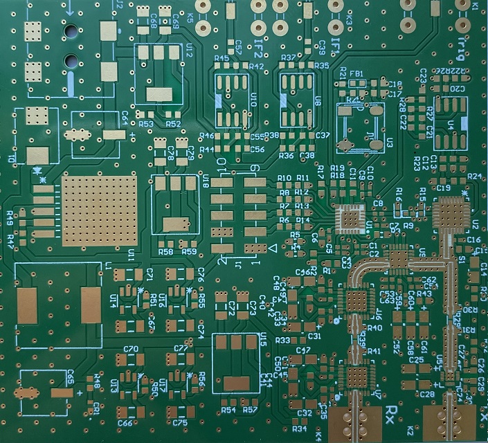
High-Speed PCBs are essential for networking switches, routers, optical communication systems, wireless infrastructure, and data transmission equipment.
They support high-speed interfaces and large data volumes while maintaining signal integrity across complex multilayer structures.
5G and Wireless Communication
Modern 5G infrastructure uses high-frequency and high-speed circuits for base stations, antennas, RF modules, and data-processing equipment.
These applications require careful control of:
- Loss
- Impedance
- EMI
- Thermal performance
- Material properties
Data Centers and AI Computing
The growth of AI and high-performance computing is increasing demand for high-speed boards supporting:
- High-speed memory
- Network interfaces
- GPU interconnects
- Storage systems
- Server backplanes
- Accelerator boards
As data rates increase, signal integrity and power integrity become increasingly important.
Automotive Electronics
Modern vehicles use high-speed communication for:
- ADAS
- Camera systems
- Radar
- Automotive Ethernet
- Infotainment
- Domain controllers
- Vehicle networking
High-speed automotive PCB designs must balance electrical performance with vibration, thermal, and reliability requirements.
Aerospace and Defense
High-speed PCBs are used in:
- Avionics
- Radar
- Navigation
- Communications
- Flight-control electronics
- Satellite systems
These applications can require specialized materials and extensive environmental and reliability testing.
Medical Equipment
High-speed PCB technology supports data-intensive medical systems including:
- Imaging equipment
- Ultrasound
- Patient monitoring
- Diagnostic instruments
- Medical networking systems
Signal accuracy and system stability are critical in these applications.
Industrial Automation
Industrial systems use high-speed PCBs for:
- Sensors
- Machine vision
- Industrial Ethernet
- Motion controllers
- Data acquisition
- Robotics
High-Speed PCB Design Best Practices
Keep High-Speed Traces Short
Reducing trace length can minimize loss, delay, and exposure to noise.
Maintain a Continuous Return Path
Avoid routing high-speed traces across gaps or splits in the reference plane.
Match Differential Pairs
Differential signals should maintain appropriate:
- Trace width
- Pair spacing
- Length matching
- Reference-plane relationship
Avoid Unnecessary Layer Changes
Every layer transition can introduce discontinuities.
Use vias carefully and optimize transitions for the interface’s electrical requirements.
Control Impedance During Design
Do not wait until manufacturing to determine whether the traces meet the required impedance.
The stack-up and trace geometry should be calculated before routing.
Separate High-Speed and Noisy Circuits
Keep sensitive analog, RF, and high-speed digital circuits appropriately separated according to the system architecture.
Use Proper Decoupling
Place decoupling capacitors close to device power pins and minimize current-loop area.
Perform SI/PI Simulation
For demanding designs, signal-integrity and power-integrity simulation can identify potential issues before fabrication.
Future Trends in High-Speed PCB Technology
Low-Loss PCB Materials
As signaling speeds increase, advanced low-loss dielectric materials will become increasingly important.
Materials based on advanced hydrocarbon, PTFE, LCP, and other low-loss systems may be used where conventional FR-4 cannot meet electrical requirements.
AI-Assisted PCB Design
AI and machine-learning tools are increasingly being integrated into EDA workflows.
Potential applications include:
- Automated routing
- Signal-integrity analysis
- Stack-up optimization
- Constraint management
- DFM checking
- Thermal analysis
AI should complement engineering judgment rather than replace system-level design expertise.
5G and Beyond
Higher communication frequencies and greater data volumes will continue to increase requirements for low-loss, high-frequency, and high-speed PCB technology.
AI and High-Performance Computing
AI accelerators, networking equipment, GPUs, and high-speed memory interfaces are creating greater demand for high-speed PCB manufacturing with tighter electrical and manufacturing control.
Advanced Packaging and HDI
The continued miniaturization of electronics will drive adoption of:
- HDI
- Microvias
- Any-layer interconnects
- Fine-line structures
- Advanced substrate-like PCB technologies
Kingda High-Speed PCB Manufacturing and PCBA Solutions
For companies developing high-speed electronics, selecting a supplier with both PCB fabrication and PCBA capabilities can simplify engineering and production management.
Kingda’s published capabilities include high-speed PCB, high-frequency PCB, HDI PCB, multilayer PCB, controlled-impedance PCB, flexible PCB, rigid-flex PCB, heavy copper PCB, and metal-core PCB assembly. (GOPCBA)
High-Speed PCB and High-Frequency PCB Capability
Kingda specifically lists high-speed and high-frequency PCB manufacturing within its technical capabilities and showcases high-speed communication backplane PCB products. (GOPCBA)
This is particularly relevant for applications involving:
- High-speed networking
- Communication equipment
- AI computing
- Industrial data acquisition
- Automotive electronics
- RF systems
Controlled-Impedance Engineering
For high-speed designs, impedance control must be considered during PCB design and manufacturing.
Kingda provides engineering support around PCB design, DFM/DFA, stack-up, manufacturing optimization, and controlled-impedance requirements. Its technical resources also address impedance mismatch and its effect on signal integrity. (GOPCBA)
Advanced SMT Assembly
High-speed boards increasingly use fine-pitch packages and complex component configurations.
Kingda’s published SMT capabilities include support for 01005 components, 0.35 mm-pitch BGA, BGA, QFN, CSP, LGA, PoP, double-sided SMT, and lead-free/RoHS-compliant assembly. (GOPCBA)
Comprehensive Testing
Kingda’s quality process includes:
IQC → SPI → SMT/THT Assembly → AOI → X-Ray → ICT/FCT → OQC
Its published inspection capabilities include 3D SPI, AOI, X-ray inspection, FAI, ICT, and functional testing. (GOPCBA)
For high-speed projects, appropriate electrical validation can be added according to the customer’s requirements.
Engineering and DFM/DFA Support
Kingda’s engineering services include:
- DFM review
- DFA analysis
- BOM verification
- Gerber review
- Pick-and-place verification
- Component availability analysis
- Alternative component recommendations
- Prototype manufacturing support
- Mass-production process optimization (GOPCBA)
Early engineering review helps identify potential manufacturing problems before they become costly redesigns.
One-Stop PCB and PCBA Manufacturing
Kingda integrates PCB design and fabrication, component procurement, SMT, DIP, finished-product assembly, and testing under a single manufacturing system. (GOPCBA)
This one-stop model can be particularly useful for high-speed products where PCB fabrication, electrical performance, assembly, and testing need to be closely coordinated.
Quality Management
Kingda states that it holds IATF 16949:2016, ISO 13485:2016, and ISO 9001:2015 certifications, with additional qualifications including ISO 14001 and UL listed on its site. (GOPCBA)
Prototype to Volume Production
Kingda supports rapid PCBA prototyping, low-volume production, and high-volume production, allowing customers to move from initial engineering boards to production through the same manufacturing partner. (GOPCBA)
Conclusion
High-Speed PCB technology is fundamental to modern electronic systems that need to transmit large amounts of data quickly and reliably.
Unlike conventional PCB design, high-speed electronics require careful management of signal integrity, impedance, crosstalk, EMI, power integrity, thermal performance, and return-current paths.
The key to successful high-speed PCB development is an integrated approach:
Material Selection + Stack-Up Design + Controlled Impedance + SI/PI Analysis + Optimized Routing + Precision Manufacturing + Comprehensive Testing
High-speed PCB technology will continue to evolve as AI computing, 5G and advanced wireless communication, automotive electronics, high-performance computing, medical imaging, industrial automation, and other data-intensive systems become increasingly sophisticated.
For companies seeking a reliable high-speed PCB manufacturer and PCBA partner, Kingda provides integrated high-speed PCB, high-frequency PCB, HDI PCB, controlled-impedance PCB fabrication, SMT/THT assembly, DFM/DFA engineering, component sourcing, inspection, and testing. (GOPCBA)
By combining PCB engineering and manufacturing with assembly and quality-control capabilities, Kingda can help customers move high-speed electronic products from prototype development to stable production.