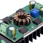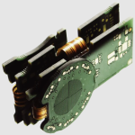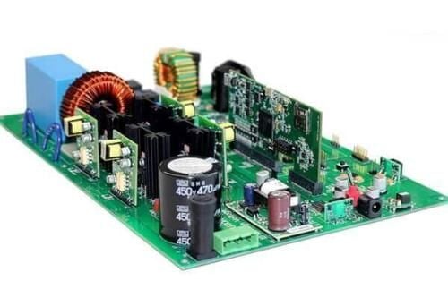
What Is an Inverter PCB?
An Inverter PCB is the printed circuit board used in an inverter system that converts direct current (DC) into alternating current (AC). Depending on the application, an inverter may convert DC power from batteries, solar panels, fuel cells, or other DC sources into a stable AC output such as 220 V, 50 Hz power for residential and industrial equipment.
A typical inverter consists of several functional sections, including the power switching stage, gate-drive circuit, control logic, protection circuit, DC-link components, and output filtering network. The PCB provides the electrical connections and physical platform required to integrate these circuits while maintaining appropriate electrical isolation, thermal performance, and mechanical reliability.
Inverter systems are widely used in household appliances, renewable-energy systems, electric vehicles, backup power supplies, industrial equipment, and portable power systems. Depending on the power rating and application, an inverter PCB may need to handle high current, high voltage, rapid switching transients, and significant heat generation.
For example, automotive inverters can be connected to a vehicle battery to supply AC power to electrical equipment during travel, field operations, or emergency situations. Low-power vehicle inverters may draw power through a cigarette-lighter socket, while higher-power systems generally connect directly to the battery through appropriately sized cables and protection devices.
The performance of the Inverter Circuit Board directly affects the conversion efficiency, output waveform, electromagnetic compatibility, thermal performance, and overall reliability of the inverter.
Applications and Advantages of Inverter PCBs
The main function of an Inverter PCB is to provide reliable control and power conversion between DC and AC systems. Its applications cover a wide range of industries.
Key advantages and applications include:
- DC-to-AC power conversion: An inverter PCB enables DC sources such as batteries, photovoltaic modules, and fuel cells to supply AC loads.
- Portable power supply: Compact inverter systems can provide AC power for laptops, electronic instruments, communication equipment, and other devices in locations without access to the grid.
- Renewable-energy integration: In solar and wind power systems, inverter PCBs are essential for converting generated DC or variable electrical energy into usable AC power.
- Automotive applications: Vehicle-mounted inverters can provide AC power for electrical tools, appliances, and emergency equipment.
- Backup power systems: Inverters can work with battery storage systems to provide backup power during grid interruptions.
- Industrial applications: High-power inverter systems are commonly used for motor drives, pumps, fans, compressors, and industrial automation equipment.
- Energy efficiency: Modern inverter designs can improve energy conversion efficiency and reduce unnecessary power losses compared with older conversion architectures.
- Low-noise operation: When properly designed, electronic inverter systems can reduce the fuel consumption and mechanical noise associated with conventional generator systems.
Common Applications of Inverter Circuit Boards
An Inverter Circuit Board can be found in many different electrical and electronic systems.
Typical applications include:
- Solar photovoltaic power systems
- Energy storage systems
- Electric vehicles and hybrid vehicles
- Automotive power inverters
- Uninterruptible power supplies (UPS)
- Industrial motor drives
- Wind power generation systems
- Portable power stations
- Household appliances
- Battery backup systems
- Marine electrical systems
- Industrial automation equipment
The required PCB structure varies considerably according to the voltage, current, switching frequency, power level, environmental conditions, and control architecture of the application.
Key Considerations for Inverter PCB Design
Designing a reliable Power Electronics PCB requires more than simply connecting the components according to the schematic. High-power inverter systems must simultaneously address electrical, thermal, mechanical, electromagnetic, and safety requirements.
Selecting the Appropriate Power Switching Device
The first important decision is selecting the appropriate power semiconductor technology. The switching device determines the required gate-drive architecture, switching frequency, thermal design, voltage rating, current capability, and PCB layout strategy.
Common power-switching technologies include:
- Silicon MOSFETs: Suitable for many low- and medium-voltage switching applications and generally offer fast switching performance.
- IGBTs: Widely used in medium- and high-power applications because of their high voltage and current handling capability.
- SiC devices: Silicon carbide MOSFETs offer high breakdown voltage, low switching losses, and high-temperature capability, making them attractive for high-efficiency inverter systems.
- GaN devices: Gallium nitride devices support very high switching frequencies and low switching losses, making them useful in compact, high-frequency power-conversion systems.
The appropriate device should be selected based on the actual operating voltage, current, switching frequency, thermal conditions, efficiency target, and cost requirements.
Evaluating Operating Voltage
Voltage rating is another critical consideration in inverter PCB design.
Designers need to evaluate the maximum operating voltage as well as transient voltages generated during switching. Power semiconductor devices and gate drivers must have sufficient voltage ratings and appropriate protection margins.
High-voltage inverter circuits may experience voltage overshoot caused by parasitic inductance, switching transients, or inadequate layout. Excessive voltage stress can damage semiconductor devices and reduce long-term reliability.
Appropriate protection mechanisms may include:
- Overvoltage protection
- Desaturation detection
- Gate-source voltage protection
- Active or passive clamping
- Snubber circuits
- Proper gate resistance
- Controlled switching speed
- Short-circuit protection
Careful PCB Layout is equally important because reducing high-current loop inductance can significantly reduce voltage overshoot and electromagnetic interference.
Considering the Application Environment
The required design approach depends heavily on the application.
For example, an industrial motor inverter operating under relatively predictable conditions may prioritize continuous thermal performance and long-term reliability. In contrast, an electric vehicle traction inverter may experience rapid load changes, vibration, temperature cycling, regenerative braking, and severe electrical transients.
Therefore, the design should consider:
- Operating temperature
- Humidity and contamination
- Vibration and mechanical shock
- Electrical transients
- Load variations
- Short-circuit conditions
- Cooling method
- Electromagnetic compatibility
- Required service life
A well-designed inverter PCB should maintain stable performance under both normal and abnormal operating conditions.
Designing the Gate-Drive and Secondary-Side Power Supply
The gate-drive circuit is critical to the operation of power semiconductor devices. The driver must provide appropriate gate voltage, sufficient drive current, controlled switching speed, and reliable isolation where required.
Half-bridge and full-bridge topologies require particular attention to high-side and low-side gate-drive power supplies. Depending on the architecture, designers may use isolated power supplies, bootstrap circuits, isolated gate drivers, or other appropriate solutions.
The gate-drive loop should be kept short and low-inductance. Gate-drive traces should also be routed away from sensitive analog and control signals to minimize unwanted coupling.
Best Practices for Inverter PCB Layout
A carefully planned PCB Layout can significantly improve inverter efficiency, switching performance, thermal management, and electromagnetic compatibility.
1. Place Critical Components First
Components with fixed mechanical positions or critical electrical functions should be placed first.
These may include:
- Mounting holes
- Connectors
- Power semiconductor devices
- Transformers
- Inductors
- Capacitors
- Heat sinks
- Current sensors
- Gate drivers
The layout should follow the principle of placing critical and mechanically constrained components first, followed by less critical components.
2. Minimize High-Current Loops
High-current paths should be as short and wide as practical.
Reducing the physical loop area of high di/dt current paths helps minimize parasitic inductance, voltage overshoot, ringing, and EMI.
Particular attention should be given to the switching loop consisting of the power semiconductor, DC-link capacitor, and associated return path.
The DC-link capacitor should be placed as close as possible to the power switching devices to reduce the effective current-loop inductance.
3. Separate High-Voltage and Low-Voltage Circuits
High-voltage and high-current circuits should be physically separated from low-voltage control and sensing circuits.
Appropriate creepage and clearance distances must be maintained according to the applicable safety standards and system voltage.
Sensitive analog signals, current-sensing circuits, feedback networks, and communication interfaces should be kept away from high-frequency switching nodes.
4. Optimize Thermal Management
Thermal design is one of the most important considerations for a high-power Power Electronics PCB.
Heat-generating components such as MOSFETs, IGBTs, diodes, inductors, transformers, and power resistors should be positioned to facilitate heat dissipation.
Depending on the power level, thermal management may involve:
- Copper planes
- Thermal vias
- Heat sinks
- Forced-air cooling
- Liquid cooling
- Metal-core PCB structures
- Thermally conductive interface materials
Temperature-sensitive components should be placed away from major heat sources.
5. Position Decoupling Capacitors Correctly
Decoupling and bypass capacitors should be located close to the corresponding power pins or switching devices.
A long connection between the capacitor and switching device increases parasitic inductance and can reduce the effectiveness of high-frequency decoupling.
For gate drivers and control ICs, short power and ground connections are particularly important.
6. Keep Sensitive Signals Away from Switching Nodes
High-frequency switching nodes can generate significant electric and magnetic fields.
Sensitive signal traces should therefore be routed away from:
- Power switching nodes
- High-current traces
- Transformers
- Inductors
- Gate-drive loops
- High-frequency clocks
Analog and digital circuits should also be separated when necessary, while grounding and return-current paths should be carefully controlled.
7. Optimize Magnetic Component Placement
Inductors and transformers should be positioned carefully to minimize unwanted magnetic coupling.
Two inductors or magnetic components should not be placed unnecessarily close and parallel to each other. If their magnetic fields interact, unwanted induced signals and electromagnetic interference may occur.
Where possible, magnetic components can be arranged with appropriate spacing or orientation to reduce mutual coupling.
8. Maintain Symmetrical Routing
Differential circuits, voltage-divider networks, current-sensing circuits, and repeated functional blocks should use symmetrical placement and routing whenever practical.
Matched trace lengths and consistent routing geometry can help improve measurement accuracy and reduce timing or common-mode errors in sensitive circuits.
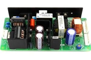
Classification of Photovoltaic Inverter PCBs
A Solar Inverter PCB is a critical part of a photovoltaic power-conversion system. A typical photovoltaic system may include solar panels, a photovoltaic inverter, an energy-storage system, a controller, and associated protection equipment.
The inverter converts DC power generated by photovoltaic modules into AC power suitable for local loads, energy storage, or grid connection.
Photovoltaic inverter PCBs can be classified according to several characteristics.
Classification by Output Frequency
Based on operating frequency, inverter systems can generally be categorized as:
- Power-frequency inverters: Typically operate around 50 or 60 Hz.
- Medium-frequency inverters: Operate at frequencies higher than conventional power frequency.
- High-frequency inverters: Use high-frequency switching to reduce the size of magnetic components and improve power density.
The exact operating frequency depends on the inverter topology and application.
Classification by Number of AC Phases
According to the AC output configuration, photovoltaic inverter systems can be divided into:
- Single-phase inverters
- Three-phase inverters
- Multiphase inverter systems
Single-phase systems are common in residential applications, while three-phase systems are widely used in commercial, industrial, and utility-scale applications.
Classification by Main Circuit Topology
Common inverter topologies include:
- Single-ended inverters
- Half-bridge inverters
- Full-bridge inverters
- Push-pull inverters
- Multilevel inverter topologies
The selected topology affects switching losses, output quality, component count, voltage utilization, and control complexity.
Classification by Power Level
Inverter systems can also be classified according to their rated power:
- Low-power inverter: Less than 1 kW
- Medium-power inverter: Approximately 1–10 kW
- High-power inverter: More than 10 kW
The exact classification may vary between manufacturers and application sectors.
Key Requirements for Photovoltaic Inverter PCBs
A Photovoltaic Inverter must provide stable and reliable power conversion despite changes in solar irradiation, load conditions, ambient temperature, and DC input voltage.
Stable Output Voltage
A photovoltaic inverter should maintain its AC output within an appropriate voltage tolerance under normal operating conditions.
The control system continuously monitors the output and adjusts switching behavior to compensate for input or load variations.
Stable voltage is particularly important for sensitive electrical and electronic equipment.
Low Waveform Distortion
Output waveform quality is another important performance indicator.
A well-designed inverter should produce an AC waveform with low total harmonic distortion (THD). Excessive harmonic distortion can cause additional heating, acoustic noise, electromagnetic interference, and reduced efficiency in connected equipment.
Modern inverter systems typically use advanced PWM control and output filtering to produce a waveform close to a sinusoidal AC signal.
Stable Output Frequency
For grid-connected and AC motor applications, output frequency must be accurately controlled.
In regions where the standard AC frequency is 50 Hz or 60 Hz, the inverter control system must maintain the appropriate frequency according to the application and grid requirements.
Frequency instability can affect motor performance, equipment efficiency, and system reliability.
Protection and Safety
In addition to voltage and frequency regulation, photovoltaic inverter systems require comprehensive protection.
Typical protection functions include:
- Overvoltage protection
- Overcurrent protection
- Short-circuit protection
- Overtemperature protection
- Reverse-polarity protection
- Surge protection
- Ground-fault protection
- Isolation monitoring
- Overload protection
These functions help prevent component damage and improve overall system safety.
Materials for Inverter PCBs
Material selection has a significant impact on the reliability of an inverter PCB.
For conventional inverter applications, FR-4 remains a widely used PCB material. However, high-power and high-temperature applications may require specialized materials or advanced thermal structures.
Important material-selection factors include:
- Glass transition temperature (Tg)
- Thermal conductivity
- Dielectric strength
- Coefficient of thermal expansion (CTE)
- Copper thickness
- Mechanical strength
- Operating temperature
- Moisture resistance
- Long-term reliability
For high-power applications, thick-copper PCB technology can be used to improve current-carrying capability and reduce conductor resistance.
Why Ceramic PCB Can Be Used in High-Power Inverter Applications
Ceramic PCB technology is particularly attractive for applications requiring high thermal performance, electrical insulation, and dimensional stability.
Common ceramic PCB substrates include aluminum oxide (Al₂O₃), aluminum nitride (AlN), and other advanced ceramic materials.
Excellent Electrical Insulation
Ceramic substrates provide excellent electrical insulation and high dielectric strength.
This characteristic makes ceramic PCB technology suitable for high-voltage and high-power electronic applications where electrical isolation is essential.
Excellent Thermal Performance
Ceramic materials generally provide significantly better thermal conductivity than conventional organic PCB substrates.
This allows heat generated by power semiconductor devices to be transferred more efficiently to heat sinks or other cooling structures.
Aluminum nitride, for example, combines high thermal conductivity with good electrical insulation, making it attractive for demanding power-electronics applications.
Good Thermal Expansion Compatibility
The coefficient of thermal expansion of ceramic materials can be relatively close to that of semiconductor materials.
This can reduce mechanical stress caused by repeated temperature changes and improve the reliability of solder joints and semiconductor interconnections.
High-Temperature Reliability
Ceramic substrates can withstand high operating temperatures and demanding thermal cycles.
For applications such as photovoltaic inverters, electric vehicle power electronics, industrial motor drives, and high-power conversion equipment, this can provide an important reliability advantage.
However, ceramic PCB is not automatically the best material for every inverter. Material selection should be based on power density, voltage, current, thermal requirements, mechanical design, production technology, and total system cost.
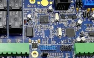
Kingda Inverter PCB Manufacturing Capabilities
For demanding inverter applications, PCB manufacturing quality is closely related to the reliability of the final power-conversion system.
Kingda can support inverter PCB projects with manufacturing considerations such as:
- Multilayer PCB manufacturing
- High-current PCB solutions
- Thick-copper PCB technology
- High-Tg materials
- High-frequency PCB solutions
- Thermal management structures
- Metal-based PCB solutions
- Rigid-flex PCB manufacturing
- Controlled impedance requirements
- Fine-line and high-density PCB fabrication
- Prototype and volume production support
For high-power inverter projects, PCB design and manufacturing requirements should be evaluated together from the beginning. Factors such as copper thickness, layer stack-up, current distribution, thermal dissipation, creepage and clearance, via design, material selection, and manufacturing tolerances can all affect the final product.
By combining appropriate PCB materials, optimized circuit architecture, controlled manufacturing processes, and careful PCB Layout, designers can achieve better electrical performance, thermal reliability, and long-term stability.
Conclusion
An Inverter PCB is a key component in modern power-conversion systems, enabling DC sources to supply stable AC power for residential, industrial, automotive, and renewable-energy applications.
Reliable inverter PCB design requires careful selection of power semiconductor devices, operating voltage, gate-drive architecture, PCB materials, thermal management methods, protection circuits, and layout strategies.
For solar and energy-storage applications, a Solar Inverter PCB must also withstand fluctuating input conditions, temperature variations, high switching currents, and long-term outdoor operation.
As power density and switching frequencies continue to increase, technologies such as SiC, GaN, thick-copper PCBs, advanced thermal structures, and Ceramic PCB substrates are becoming increasingly important.
Working with an experienced PCB manufacturer such as Kingda can help ensure that the PCB manufacturing process is aligned with the electrical, thermal, mechanical, and reliability requirements of the inverter system.