Laser Direct Imaging: Why Fine-Line Boards Depend On It
Laser direct imaging has quietly become the technique that decides whether a fine-line design can be manufactured at all. Where a design calls for conductors and spaces measured in tens of microns, the traditional photographic process is at the edge of what it can hold, and the layer-to-layer registration that the design assumes is difficult to guarantee. Understanding what the imaging step does explains why line width is a manufacturing constraint rather than only a layout preference.
What the Imaging Step Does
Before copper can be etched, the pattern must be transferred to a resist that protects the copper that is to remain. In the classic process, that transfer is done photographically: the board is coated with a photosensitive resist, a film carrying the pattern is aligned to the board, and the resist is exposed through the film. The exposed or unexposed areas are then developed away, and the copper underneath them is etched or plated. The phototool, the film carrying the pattern, is the part of that sequence that determines how fine a feature can be reproduced.
The limitation is the film. A phototool has dimensional stability that depends on temperature and humidity, and it wears with use. It also has to be aligned mechanically, so the achievable registration between layers is bounded by the mechanical alignment system. As feature sizes shrink, both effects consume a larger share of the tolerance budget.
How Direct Imaging Differs
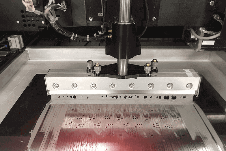
Laser direct imaging removes the film. The pattern is written onto the resist by a laser or an array of lasers that is controlled from the same digital data used to generate the artwork, so there is no physical tool to align, and the image can be scaled or distorted to match the panel before it is written.
That last point matters more than it first appears. A panel that has expanded during lamination is no longer the size it was designed to be. A photographic tool cannot compensate; a direct imaging system can apply a scaling factor to each panel, which recovers registration that would otherwise have to be absorbed by design margins. This is why direct imaging is associated with improved layer-to-layer alignment as much as with finer lines, and why it replaced the film-based transfer in the panels where registration is the limiting factor.
Fine Lines and the Resist
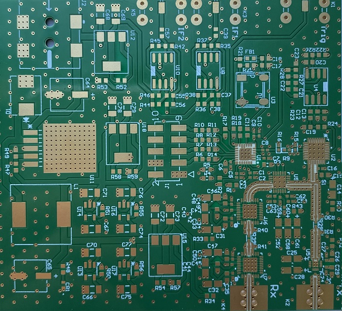
Imaging limits are not only a matter of the exposure system. The resist has to resolve the pattern, which means its thickness, its adhesion to the copper and its development characteristics all constrain the minimum feature. Direct imaging allows a thinner, higher-resolution resist to be used in a controlled way, because the exposure dose can be tuned per panel rather than fixed by a film.
The practical result is that features below roughly thirty microns of line and space become feasible. That is the region in which fine-pitch ball grid array packages and high-density interconnect designs operate, and it is why the technique became necessary rather than merely desirable. Inkjet printing is the other route being developed for the same purpose, with the advantage of adding material rather than removing it. Our imaging system notes describe the wider process.
<img src="https://www.gopcba.com/wp-content/uploads/2026/09/219.png" alt="Fine line circuit pattern on a high density interconnect PCB layer” />
Registration and Layer Count
Registration between layers is a stack of tolerances: the inner layer pattern position, the lamination shift, the drill position and the imaging alignment. Every one of those adds to the total, and the design has to leave enough margin around a via for the cumulative error. Improving any single term allows the margin to shrink, which allows a design to fit into fewer layers or to accommodate a finer pitch.
Direct imaging improves the imaging term and, through panel scaling, part of the lamination term as well. That is why the technology is often adopted together with a layer count reduction: the same design that could not be routed on eight layers with photographic imaging becomes routable when the annular ring requirement is relaxed.
Yield and the Economics
The economic case for direct imaging is not the cost per panel but the yield. A process that holds a tight registration tolerance produces fewer scrapped panels, and the value of a scrapped multilayer panel near the end of the process is much higher than the value of the raw material. For a design with fine features or many layers, the improvement in yield usually outweighs the higher imaging cost.
There is also a flexibility argument. Because the pattern is data rather than film, a change to the artwork does not require a new tool, and the setup time for a new design is short. That matters for prototype and small-batch production, where the tooling cost of a photographic process is spread over few boards.
Implications for the Designer
The designer’s obligation is to know which imaging process the chosen fabricator will use, because the minimum line width, the minimum annular ring and the achievable registration all follow from it. A design that specifies the smallest features the layout tool allows, without reference to the fabrication process, will be quoted at a premium or returned for revision. A design that matches its geometry to a known process gets a predictable result.
Our design release checklist covers the geometry checks, the cost reduction notes explain how a feature size decision appears in a quotation, and the layer assignment guidance describes how registration margins influence the stack-up.
Where Direct Imaging Fits in the Line
Direct imaging is normally applied to the outer layers, where the smallest features usually appear and where the registration to the drilled holes matters most. Inner layers may be imaged photographically or directly, depending on the design and the fabricator. Because the data path is the same as the one used to generate the artwork, the imaging step also provides a convenient point at which the panel can be measured and scaled before exposure, which is how the registration improvement is realised in practice.
FAQ
Does direct imaging mean the design can use any line width? No. It raises the resolution limit but does not remove it, and the limit applies to the whole process rather than to the imaging step alone. Etching, plating and the resist all have their own minimum features. The practical minimum is the largest of those limits, and it should be confirmed with the fabricator rather than assumed from the imaging capability.
Why does registration matter more on a multilayer board? Because every via has to connect to a pad on an inner layer, and the tolerance between the pad and the hole is the sum of the errors accumulated from that layer to the outer surface. On a two-layer board the chain is short; on a ten-layer board it is long. The annular ring requirement therefore grows with the layer count unless the registration process is improved to compensate.
What does gopcb need to know about feature sizes? The minimum line width and spacing, the minimum annular ring, and which of those are driven by electrical requirements as opposed to habit. We review those against the process that will be used for the panel, so that the quotation and the delivery date are based on geometry the process can actually hold.