PCB Layout Component Spacing Rules and Twelve Practical Checks
Most assembly problems that reach the production line were decided months earlier on the layout screen. A part placed 0.1 mm too close to its neighbour turns a normal stencil print into a bridging defect; a thermal pad connected to a copper flood with four solid spokes becomes a rework nightmare. The rules below are the ones that pay back the most and that a design rule check cannot always catch on its own.
Component Spacing on SMT Assemblies
The starting point is component spacing on the printed circuit board itself. Two parts of the same type and height are usually safe at 0.3 mm or more between bodies. For parts of different heights the gap has to scale with the difference, because the stencil and the placement nozzle both need clearance: a working rule is 0.13 times the height difference plus 0.3 mm. Components that will only ever be soldered by hand need at least 1.5 mm, since an iron has to fit between them without touching a neighbour.
Spacing is not just about placement. Solder paste printing, reflow and inspection all need room. The most common consequence of tight spacing is that after reflow the placement nozzle touches a tall neighbour and pushes an already placed part out of position. Reviewing the placement against the paste stencil openings before releasing the design catches most of this.
SMD to Through-Hole Distance
Where a through-hole part sits next to a surface mount device, keep the distance in the 1 to 3 mm range. The pin and the wave or selective solder nozzle need clearance, and a lead that passes too close to a chip package can wick solder into places it does not belong. Through-hole parts are less common than they once were, but connectors, relays and large capacitors still appear on most boards and still need the space.
Mixed technology also affects the assembly sequence. If the through-hole parts are soldered after the surface mount reflow, the wave or selective solder fixture needs a clear approach path and the adjacent SMD parts may need to be masked. Planning the placement with that sequence in mind avoids a fixture that cannot physically reach the pins.
Decoupling Capacitor Placement
Every decoupling capacitor belongs as close as possible to the power pin it serves, on the same side of the board as the package where the routing allows. When a device has several supply pins, each one gets its own capacitor rather than sharing one across the package. The loop area formed by the capacitor, the via and the pin decides how well it works at high frequency, so a capacitor that is electrically close but routed through a long stub is no better than one placed far away.

Bulk capacitance is a separate function. A large electrolytic or polymer capacitor near the regulator handles slow load steps, while the small ceramic parts at the pins handle the fast edges. Confusing the two roles leads to a layout that has plenty of capacitance but still fails a load step test, because the charge is stored too far from the point of use.
Parts Near the Board Edge
Components near the panel edge have to satisfy two conditions. They should be oriented parallel to the separation direction so that the mechanical stress of depanelisation is spread evenly; a part placed across the cut line can lose one pad before the other and lift off the board. There should also be a keep-out band along the edge where no components are placed at all, typically 3 to 5 mm depending on the depanelisation method. The rules for the outline and its mounting features are covered in board outline and mounting design.
Thermal Relief on Copper Floods
A pad that lands in a copper flood should be connected through a thermal relief rather than a solid connection. Four narrow spokes keep the pad electrically connected while limiting heat conduction into the plane, so a soldering iron can bring the joint up to temperature. A solid connection spreads heat so effectively that hand soldering and desoldering become impractical. The number of spokes and their width also set the current carrying capacity, so a power pad needs wider or more numerous connections than a signal pad.
Teardrops and Pad to Trace Match
Where a trace is narrower than the through-hole pad it enters, a teardrop is a cheap improvement. The tapered transition reduces the impedance step that a sudden width change creates, prevents the trace from cracking at the pad when the board flexes, and improves the etch yield because a thin trace meeting a round pad is exactly the geometry that breaks during development. The two traces leaving a two-terminal pad should also be the same width and leave at the same angle, so the pad is loaded symmetrically.
Unused Pins and Grounding
Unused device pins still exist on the package, and leaving their pads floating is a common source of noise pickup. Keep the pad in the footprint, connect it to ground where the datasheet allows, and use the pad as a shield. Leaving the pin unconnected but ungrounded means a short stub attached to a sensitive input, which is the worst of both options. Pad geometry and land pattern choices are described in the notes on PCB pad design standards.
Vias and Via in Pad
A through via placed directly on a solder pad will wick paste away from the joint during reflow and leave a void or a partial joint. Move the via off the pad and connect it with a short stub, or use a filled and plated via in pad structure when the density leaves no alternative. If the via must stay in the pad, it has to be plugged and planarised, and the stencil aperture has to be adjusted for the reduced paste volume. Current carrying rules for the traces that connect these structures are covered in trace width and current calculation.
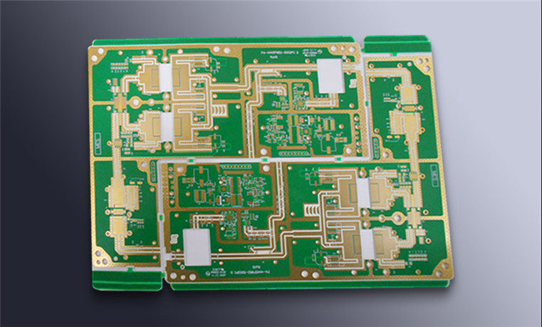
Vias that are not in pads deserve a rule of their own. Tented vias are fine on low density boards, but a via that sits under a component body should be plugged so that flux and cleaning agents do not become trapped against the package. On fine pitch devices, a via placed between two pads can also steal paste through the stencil if the aperture spacing is tight, so the via should be moved off the pad row entirely.
Electrolytic Capacitors and Heat Sources
Electrolytic capacitors age quickly when they run hot, so place them away from regulators, power resistors and other heat sources, and check the ambient temperature on the datasheet against the local board temperature rather than the room temperature. Where space is tight, orient the capacitor so that its body is not in the shadow of a hot component, and consider a polymer type where the expected life matters more than the cost difference.
FAQ
What is the minimum component spacing for a double sided assembly? About 0.3 mm between bodies of equal height is a practical floor for machine placement, but the nozzle and stencil requirements of the specific parts should be checked first.
Should thermal relief spokes be used on ground pads of a power device? Only where hand soldering or rework is expected. A solid connection is better for current and heat spreading, so the choice depends on which requirement dominates.
Is via in pad always better than a via next to the pad? No. It costs more because the via has to be filled and plated flat. Use it when escape routing or loop inductance forces the via inside the land.