Metal Core PCB Insulation and Thermal Path Design
A metal core board is chosen when a component produces more heat than a glass reinforced laminate can move away. The copper circuit sits on a thin insulating layer, and beneath that layer is a solid aluminium or copper plate that spreads heat sideways and hands it to a heat sink. The insulation is the whole design problem, because it must conduct heat and block voltage at the same time.
What a Metal Core Board Is
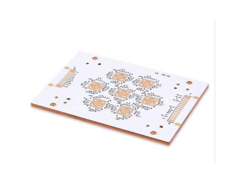
The construction is simple in principle. A sheet of aluminium or copper forms the base, a thermally conductive dielectric is coated or laminated onto it, and copper foil is bonded on top and etched into the circuit. The base plate is not connected to the circuit, so the electrical isolation is provided entirely by the dielectric layer.
Because the base is continuous metal, the board is mechanically stiff, it does not absorb moisture the way a laminate does, and it spreads heat laterally very effectively. Those properties make metal core boards a common choice for lighting, motor drives and power conversion, where the heat source is concentrated in a small area.
The Dielectric Layer Sets the Limit
The dielectric is the weakest link in the chain. It is thin, typically between 60 and 150 microns, and its thermal conductivity is far lower than the aluminium beneath it. Almost the entire temperature drop from the component to the base plate happens across this one layer, which is why its specification matters more than the base metal.
The layer must also withstand the working voltage of the circuit, so there is a direct trade off between thickness and thermal performance. A thicker dielectric raises the breakdown voltage and lowers the capacitance, but it adds thermal resistance. Selecting the layer is therefore an exercise in balancing electrical safety against thermal budget.
Thermal Path from Junction to Base
Heat leaves a component through its thermal pad, crosses the solder joint, travels through the copper island on the board surface, crosses the dielectric, and then spreads through the aluminium base before reaching the heat sink interface. Each step has a thermal resistance, and the total determines the junction temperature.
The copper island matters more than it appears. A large copper area above the dielectric gives the heat an easier entry point, and a small pad concentrates the flux so that the dielectric directly beneath it overheats. Designing the copper island as a spreader, rather than as a footprint sized pad, is the single most effective improvement in most designs.
Thermal Conductivity Numbers and Their Meaning
Dielectric materials are quoted with a thermal conductivity in watts per metre kelvin. A conventional FR4 laminate sits near 0.3, while filled dielectric films for metal core boards reach 1 to 3, and some specialised products claim higher. The number is measured through the thickness, so it is only useful when the thickness is quoted alongside it.
A more practical comparison is thermal resistance per unit area, given in square centimetres kelvin per watt. Two materials with the same conductivity but different thicknesses will not perform alike, and a thin dielectric often beats a more conductive but thicker one. Our notes on pcb laminate material properties explain how to read these figures.
Layout Rules That Shorten the Thermal Path
Give every heat generating component a copper island larger than its thermal pad, and keep that island solid rather than hatched or perforated with vias. On a metal core board vias into the base are generally not used, because the base is not part of the circuit and the isolation would be compromised. The dielectric itself is the intended thermal via.
Place the hottest components with the largest islands and keep them away from the board edges unless the edge is clamped. Where several components share one island, the heat flux adds and the dielectric under the centre of the group sees the sum. Spreading the group, or splitting it into separate islands, reduces the peak temperature.
Isolation, Breakdown and Safety Spacing
The dielectric layer is the only insulation between mains referenced circuitry and a metal base that a user may touch, so its breakdown rating is a safety parameter rather than a performance one. The rated voltage is usually quoted for a short duration test, and the continuous working voltage must be substantially lower to account for ageing and partial discharge.
Where the base is earthed, the isolation requirement is set by the applicable safety standard for the product. Where the base is exposed to touch and unearthed, the requirement is stricter and may force a thicker dielectric, a second insulation barrier or a fully enclosed design. Trace spacing on the circuit layer follows the same creepage rules as any other high voltage board.
Assembly, Mounting and the Heat Sink Interface
The interface between the base plate and whatever cooling it is attached to often has more thermal resistance than the dielectric. A machined surface with a thin, even layer of thermal compound performs far better than a rough surface with a thick pad. Screw torque should be specified and controlled, because the aluminium base deforms under uneven pressure.
Where the base itself is the heat sink, it must be large enough to dissipate the power by convection, and the fins or the mounting plane should be part of the mechanical design rather than an afterthought. Our notes on pcb thermal management design cover the interface calculations.
Materials Compared
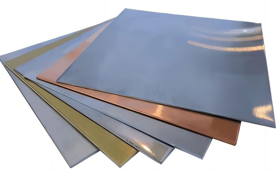
Aluminium is the default base because it is light, inexpensive and reasonably conductive. Copper bases conduct better and spread heat more evenly, but they are heavier and cost more, so they appear in high power density products where the extra spreading is worth it. Some boards use an aluminium base with a copper coin inserted directly under the hottest component.
Ceramic substrates take the opposite approach, using a very thin, very conductive insulating layer on an aluminium or copper base, or an aluminium oxide substrate with no polymer at all. They outperform metal core laminates thermally and electrically, at a higher cost and a smaller achievable board size. The comparison is set out in our guide to metal core pcb vs ceramic pcb.
Fabrication and Test Notes
Metal core boards are machined rather than punched, and the aluminium burrs at the edge have to be controlled because they can break through the dielectric. V scoring is limited, laser cutting is avoided near the dielectric, and the surface finish is usually a lead free hot air level or an immersion finish that tolerates the soldering cycle.
Testing is the same as any other board, but the base plate must be handled in a way that does not short a probe to an exposed edge. Where the design includes an isolation requirement, a hipot test between the circuit and the base is normally specified, and the test voltage and duration should be stated on the drawing together with the plating thickness from our pcb plating thickness guide.
FAQ
Can a metal core board carry mains voltage? Yes, provided the dielectric is rated for the working voltage with margin and the product standard allows the construction. The base is usually earthed and the isolation is verified by a hipot test, so the dielectric specification and the test conditions both belong on the drawing.
Why not simply use many thermal vias instead? Vias require the base to be part of the circuit or to be isolated individually, which removes the advantage of a continuous metal plate. The dielectric layer already performs the function that vias serve on an FR4 board, and it does so over a much larger area.
Does a thicker dielectric improve thermal performance? No, it does the opposite. Thicker dielectric raises the breakdown voltage but increases thermal resistance. The aim is the thinnest layer that still satisfies the isolation requirement with adequate margin for ageing.