Metallized Half-Hole PCB Manufacturing: Challenges of RO4350 and FR-4 Hybrid Lamination
A Metallized Half-Hole PCB combines electrical connectivity and signal transmission in a compact board structure, making it suitable for high-frequency communication equipment, precision testing instruments, and other advanced electronic applications. Combining RO4350 with FR-4 in a hybrid construction can provide a practical balance between high-frequency performance and manufacturing cost.
RO4350 is widely recognized for its high-frequency electrical characteristics, while FR-4 remains a widely used and cost-effective PCB substrate. A properly designed Hybrid Lamination PCB can therefore integrate the performance advantages of both materials.
However, RO4350 and FR-4 have different physical properties, thermal characteristics, resin systems, and processing requirements. When these differences are combined with the special geometry of metallized half-holes, manufacturers must carefully control lamination, dimensional accuracy, drilling, desmearing, and plating processes.
For projects that require both board fabrication and assembly, manufacturers can also integrate PCB Manufacturing with downstream assembly services to reduce process handoffs and improve overall production consistency. PCB Manufacturing
1. Layer Bonding Challenges in RO4350 and FR-4 Hybrid Lamination
One of the primary challenges of a Hybrid Lamination PCB is achieving reliable bonding between two materials with different resin systems and thermal properties.
RO4350 is engineered for high-frequency applications and has material characteristics that differ from conventional FR-4 epoxy systems. When the two materials are laminated together, differences in resin behavior and thermal expansion can create stress at the interface.
If the lamination process is not properly optimized, several problems may occur, including:
- Insufficient interlayer bonding
- Delamination
- Voids between material interfaces
- Internal stress
- Board warpage
During heating and cooling, RO4350 and FR-4 may expand and contract at different rates. These differences can generate mechanical stress within the laminated structure. If the stress is not properly managed, the interface between the two materials may become a potential point of failure.
Improving the Lamination Interface
Manufacturers can address these issues through material compatibility optimization and process control.
A compatible bonding or transition material may be considered between RO4350 and FR-4 when required by the stack-up design. The purpose is to improve interfacial adhesion and reduce the mechanical stress caused by material differences.
At the same time, lamination parameters should be carefully controlled. Heating rate, temperature profile, pressure, dwell time, and cooling conditions all need to be matched to the selected materials.
The objective is to create a uniform laminated structure with sufficient bonding strength while minimizing internal stress, voids, and warpage.
2. Dimensional Stability and Accuracy Control
Dimensional stability is particularly important for a Metallized Half-Hole PCB because half-hole structures require accurate positioning and consistent mechanical processing.
RO4350 and FR-4 can exhibit different dimensional changes during thermal processing. When the materials are laminated together, their different expansion and contraction characteristics can affect the final dimensions of the board.
Even a relatively small dimensional shift can influence subsequent drilling and routing operations.
Potential consequences include:
- Misalignment between the designed and actual hole positions
- Inconsistent half-hole geometry
- Reduced mechanical accuracy
- Difficulties during edge routing
- Poor connector alignment
- Increased manufacturing variation
Controlling Dimensional Variation
Dimensional control should begin before lamination.
The PCB manufacturer should evaluate the expected material movement and incorporate appropriate compensation into the fabrication data. Lamination conditions should also be optimized to reduce unnecessary internal stress.
Controlled heating and cooling profiles can help minimize uneven deformation. In addition, manufacturers can inspect board flatness and dimensions after lamination before proceeding to half-hole processing.
For high-precision applications, dimensional inspection at multiple stages can help identify process deviations before they affect subsequent manufacturing steps.
3. Drilling and Half-Hole Processing Challenges
The manufacturing of a Metallized Half-Hole PCB involves several specialized processes, including drilling, desmearing, copper deposition, electroplating, and edge processing.
When RO4350 and FR-4 are used in the same board, the different material characteristics can make drilling and hole-wall preparation more challenging.
During drilling, the tool interacts with different materials within the same stack-up. Changes in material properties can influence cutting conditions, tool wear, hole-wall quality, and burr formation.
If the drilling process is not optimized, manufacturers may encounter:
- Irregular hole diameters
- Rough hole walls
- Excessive burrs
- Drill bit wear
- Inconsistent half-hole geometry
- Reduced plating reliability
Optimizing the Drilling Process
The drilling parameters should be selected according to the complete material stack-up rather than treating RO4350 and FR-4 as identical materials.
Appropriate drill tools, spindle speeds, feed rates, entry materials, and backup materials should be evaluated according to the specific board construction.
When the drill passes through different material regions, stable cutting conditions are particularly important. The objective is to maintain consistent hole quality while minimizing tool wear and mechanical damage.
After drilling, the hole walls must be properly cleaned and prepared for metallization.
4. Desmearing and Surface Preparation
Desmearing is another important stage in the manufacturing of a RO4350 PCB and FR-4 PCB hybrid structure.
Drilling can leave resin residues and debris on the hole walls. These contaminants can interfere with subsequent copper deposition and reduce the reliability of the plated connection.
Because RO4350 and FR-4 have different material compositions, the desmear process must be compatible with the complete material system.
An overly aggressive treatment may damage the substrate, while insufficient treatment can leave residues that compromise copper adhesion.
Process Control for Reliable Hole Walls
A controlled surface preparation process should remove drilling residues without unnecessarily attacking the substrate.
Depending on the material combination and manufacturing requirements, chemical treatment, plasma treatment, or other suitable preparation processes may be evaluated.
The critical objective is to achieve clean, properly conditioned hole walls before electroless copper and subsequent electroplating.
For assemblies requiring SMT processing after fabrication, maintaining consistent PCB surface quality is equally important because board quality directly affects solderability and assembly yield. Manufacturers can combine fabrication with SMT PCB Assembly when the project requires an integrated PCB production and assembly solution. SMT PCB Assembly
5. Metallization and Plating Reliability
After drilling and surface preparation, the next major challenge is establishing a reliable conductive layer inside the holes and along the half-hole structure.
A Metallized Half-Hole PCB requires consistent copper coverage to ensure reliable electrical connection. Any discontinuity, insufficient copper thickness, poor adhesion, or uneven plating can negatively affect the board’s electrical and mechanical performance.
The interface between RO4350 and FR-4 may require particular attention because differences in material behavior can influence surface preparation and copper adhesion.
Improving Plating Uniformity
Manufacturers should carefully control the electroless copper deposition and electroplating processes.
Important parameters may include:
- Copper deposition thickness
- Current density
- Plating time
- Solution chemistry
- Agitation
- Temperature
- Anode-to-cathode configuration
Uniform current distribution is particularly important when processing complex half-hole geometries.
The manufacturer should also monitor plating thickness and inspect the half-hole structure to verify that the required copper coverage has been achieved.
Where necessary, cross-sectional analysis can be used to evaluate hole-wall plating quality, copper thickness, material interfaces, and potential defects.
6. Protecting the Integrity of the Plated Half-Hole
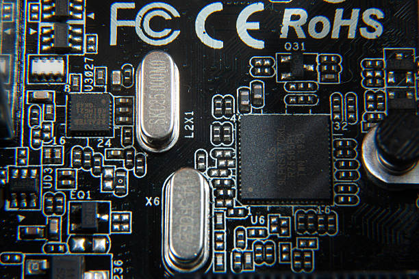
The plated half-hole is exposed to additional mechanical and environmental stresses compared with fully enclosed internal vias. As a result, plating integrity must be considered throughout the manufacturing process.
Potential reliability risks include:
- Incomplete copper coverage
- Weak copper adhesion
- Localized thin plating
- Cracks caused by mechanical stress
- Corrosion
- Contact instability
Proper cleaning and activation before plating are essential for creating a suitable surface for copper deposition.
The electroplating process should then be monitored to maintain stable copper thickness and adhesion.
For products requiring both fabrication and component sourcing, integrated manufacturing services can also simplify the supply chain. Gopcba provides Components Procurement services that can help coordinate component sourcing with PCB assembly requirements. Components Procurement
7. Inspection and Reliability Verification
Manufacturing a high-performance RO4350 PCB with FR-4 hybrid construction requires inspection throughout the production process rather than relying only on final testing.
Key inspection points may include:
Material and Lamination Inspection
The laminated structure should be checked for:
- Delamination
- Voids
- Warpage
- Layer misalignment
- Dimensional variation
Hole and Half-Hole Inspection
Drilled and processed holes should be evaluated for:
- Hole diameter
- Hole position
- Hole-wall condition
- Half-hole geometry
- Burrs
- Edge quality
Plating Inspection
Copper plating should be evaluated for:
- Plating continuity
- Copper thickness
- Adhesion
- Coverage uniformity
- Cracks or discontinuities
Cross-sectional inspection can provide additional information about the internal structure and plating quality.
8. Integrating PCB Fabrication With Assembly
For many electronic products, PCB fabrication is only one stage of the complete manufacturing process. After the board is produced, components must be mounted and soldered according to the product design.
Depending on the project, manufacturers may use SMT, through-hole, or mixed-technology assembly.
For products containing both surface-mounted and through-hole components, Mixed Technology PCB Assembly can combine different assembly methods within the same production process. Mixed Technology PCB Assembly
This integrated approach can reduce the number of supplier handoffs and simplify communication between PCB fabrication and assembly teams.
For prototype and low-volume projects, the manufacturing process can also be coordinated with Prototype PCB Assembly services to support design verification and engineering validation. Prototype PCB Assembly
9. Key Manufacturing Considerations for RO4350 and FR-4 Hybrid Boards
The successful production of a Hybrid Lamination PCB depends on controlling the interaction between material selection, lamination, machining, metallization, and inspection.
The major considerations include:
- Material compatibility – Evaluate the resin systems, thermal properties, and mechanical characteristics of RO4350 and FR-4.
- Lamination control – Optimize temperature, pressure, heating rate, dwell time, and cooling conditions.
- Dimensional compensation – Account for material movement during the PCB manufacturing process.
- Drilling optimization – Select appropriate tools and drilling parameters for the complete stack-up.
- Surface preparation – Remove drilling residues while maintaining substrate integrity.
- Plating control – Maintain consistent copper deposition and plating thickness.
- Half-hole accuracy – Ensure accurate hole positioning and edge processing.
- Inspection and testing – Verify dimensions, laminate integrity, hole quality, and copper plating reliability.
Conclusion
The production of a Metallized Half-Hole PCB using RO4350 and FR-4 hybrid construction presents several manufacturing challenges. The primary difficulties involve material compatibility, interlayer bonding, dimensional stability, drilling, desmearing, metallization, and plating reliability.
By optimizing the material stack-up, controlling the lamination process, compensating for dimensional changes, selecting suitable drilling parameters, and maintaining strict plating and inspection procedures, manufacturers can achieve more stable production results.
The combination of RO4350’s high-frequency performance and FR-4’s cost advantages makes this type of hybrid construction an attractive option for applications that require both electrical performance and cost efficiency.
A capable PCB manufacturing partner should be able to evaluate the complete process from material selection and board fabrication through inspection and assembly. With coordinated PCB Manufacturing, component sourcing, and PCB assembly capabilities, Gopcba can support a more streamlined manufacturing workflow for prototype, low-volume, and production-stage electronic products.