Multicore Processor Board Layout for Embedded Systems
A multicore processor board looks like a single core board with more pins, and that assumption is what makes the first prototypes misbehave. Several cores running at once change the current profile, the thermal load and the way peripherals contend for memory, so the layout has to be planned around concurrency from the start. This article covers the decisions that separate a stable multicore processor board from one that only works with a light workload.
Deciding What the Extra Cores Are For
Before routing, write down how the cores will be used: one for a control loop, one for communication, one for signal processing, one idle as reserve. That map determines which interfaces must be close to which core, which memory regions must be reachable with low latency, and where the interrupt load will concentrate. A board layout that ignores the software map usually ends up with one core starved while another waits on an interface placed far away.
The map also exposes the power profile. Cores that run simultaneously draw current in step, so the supply sees larger and faster transients than a single core specification suggests. Estimate the worst case load step as the sum of the cores that may start together, and size the regulators and the bulk capacitance for that number rather than for the average current in the datasheet table.
Power Delivery Network Planning
The power delivery network is the first place concurrency shows up. Current from the regulator to the die passes through planes, vias and the package, and each of those contributes inductance. Keep the loop from the regulator output to the processor supply pins as short and wide as the layout permits, and place the bulk capacitance where the current step begins rather than at the far end of the board.
Use a solid plane for each high current rail and keep the return path directly beneath it. Where two rails must share an area, separate them so that the return current of one does not flow under the other, following power plane splitting rules. Verify the result by measuring the rail at the pins during a load step, not at the regulator output where the transient has already been absorbed by the trace.
Thermal Spreading under Multi Core Load
Thermal spreading becomes a layout task once several cores run together. The heat flux through a small package area is high, so the copper directly under the thermal pad must be substantial and connected to internal planes with a dense via array, following via design rules for drill size and annular ring. A few thermal vias are not enough; the array should cover the full pad area and connect to copper on every available layer.
Plan the path from the die to the ambient as a chain: package, thermal interface, board copper, enclosure, air. A weak link anywhere in that chain limits the whole system, and the weakest link is usually the interface between the board and the enclosure. Measure case temperature under the real workload before committing to an enclosure design, because a multicore board that throttles in a sealed box has effectively reduced its own clock.
Memory Channel Routing
Multicore processors usually provide one or two memory channels, and the routing rules are the same as for any high speed bus: controlled impedance, length matching within the group, and a continuous reference plane. What changes is the bandwidth demand. Several cores accessing memory at once consume the available bandwidth quickly, so the interface must be routed to work at its rated speed rather than at a reduced rate that hides a marginal layout.
Route the data groups on a single layer where possible, keep the via pattern consistent, and match length within each byte lane. Use the techniques described for serpentine routing and length matching rather than adding delay haphazardly. Where two channels are present, keep them separated so that crosstalk between channels does not degrade the effective bandwidth.
Interrupt Routing and Peripheral Affinity
Peripherals that must respond quickly should be physically close to the core that services them, because trace length is part of the interrupt latency budget. This is not a routing preference but a system decision: an encoder input routed the long way around the board adds propagation delay, and the software has no way to remove it later.
Group high rate peripherals near the processor and keep their ground returns local. Where a peripheral must be remote, consider a serial interface with its own local processing rather than a long parallel bus, because a long parallel connection is more likely to pick up noise and harder to terminate correctly. Document the intended affinity so that the next revision does not quietly move a critical interface to the far corner of the board.
Clock and Reset Coordination
Several cores do not need several crystals, but the reference distribution still matters. Use one high quality reference for the processor and derive the peripheral clocks from buffered outputs where the device provides them, so that all domains share the same timebase and no drift appears between them. Keep the reference trace short, guarded by ground, and away from switching nodes.
Reset coordination needs the same attention. Define the reset tree explicitly: what holds the processor in reset, what the processor releases, and how the peripherals behave while the rails are settling. A peripheral that starts before its host core is configured can drive a bus that nothing is listening to, which produces errors that look intermittent in software but are entirely deterministic in hardware.
Debug and Bring-Up
Bring-up on a multicore board should be staged per core and per interface. Start with a single core running from internal memory, verify the rails and the reference clock, then enable one peripheral at a time before introducing the operating system and the full workload. This identifies whether a failure is caused by the interface itself or by contention that only appears when everything runs together.
Provide debug access that supports that staging: a serial console, a JTAG or SWD header, and test points on every rail. Route the debug signals to pads that remain accessible with the board installed in its enclosure if the product will be serviced in the field. The cost is a few square millimeters and the benefit is measured in days.
Layer Planning and Cost
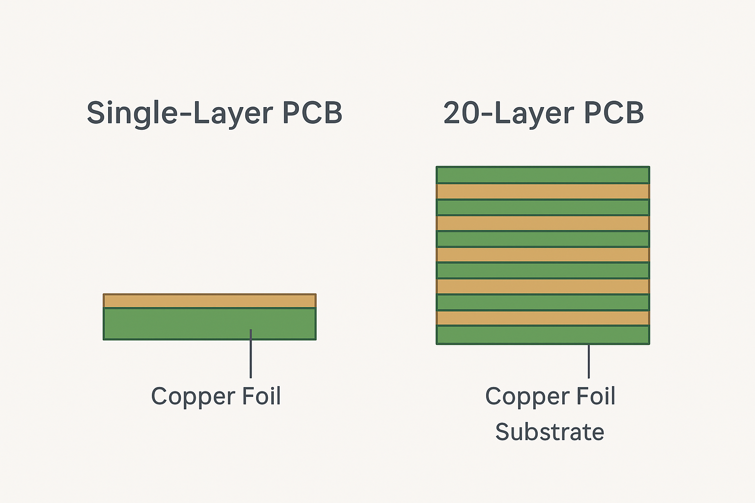
Layer count follows from the memory bus, the escape pattern and the number of power rails. Four layers is the practical minimum for a single channel device; six or eight is common when two channels and several serial links share the board. Adding a pair of layers for power and ground is almost always cheaper than routing a compromised plane structure and then debugging it.
gopcb builds processor boards up to the layer counts these devices require, and reviews the stackup, the power delivery plan and the memory routing before fabrication because those three decisions are interdependent. Correcting them after the first panel is etched costs an order of magnitude more than getting them right in the initial layout.
FAQ
Does a multicore board need more layers than a single core board? It usually does, not because of the cores themselves but because of the memory channels and the additional power rails that come with a more capable device. The escape pattern of the package is often the deciding factor.
How should the thermal pad be connected? Use a dense via array under the full pad area, tied to solid copper on the inner and bottom layers, and keep the solder void content low so the joint conducts heat rather than insulating. A large pad with few vias performs poorly regardless of its area.
What causes throughput to drop when more cores run? Memory contention and interrupt latency are the usual causes, followed by thermal throttling. Measure the interface bandwidth and the case temperature together under the real workload before assuming the software is at fault.