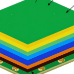
In high-speed circuit design for a Multilayer PCB, many engineers focus primarily on trace width when calculating controlled impedance. However, trace width is only one part of the transmission-line structure. The dielectric thickness, dielectric properties, copper geometry, and reference-plane configuration all influence the final impedance.
If the dielectric system is not properly defined during the design stage, a PCB may pass nominal Impedance Simulation but fail impedance verification after fabrication. This can lead to engineering changes, production delays, material waste, and additional debugging work.
For four-layer, six-layer, and higher-layer-count boards, understanding the relationship between the Dielectric Material and impedance is therefore fundamental to reliable high-speed PCB design.

1. How Dielectric Parameters Affect PCB Impedance
The impedance of a PCB transmission line is determined by its complete physical and electrical structure. For common microstrip and stripline configurations, two important dielectric parameters are the dielectric constant (Dk) and dielectric loss tangent, commonly represented by Df.
Dielectric Constant (Dk)
The Dielectric Constant (Dk) influences the electromagnetic field distribution around a signal trace.
For a given transmission-line geometry, increasing the effective Dk generally causes the characteristic impedance to decrease, while decreasing the effective Dk generally causes impedance to increase.
The actual sensitivity depends on the transmission-line structure.
For a surface microstrip, the electromagnetic field is distributed partly through the dielectric and partly through the surrounding environment. For an inner-layer stripline, the signal is enclosed by dielectric material between reference planes, making the dielectric system a particularly important part of the impedance model.
Therefore, using an inappropriate Dk value during simulation can create a significant difference between the predicted impedance and the manufactured result.
Dielectric Thickness
Dielectric thickness determines the distance between the signal conductor and its reference plane.
In many common transmission-line configurations, increasing the trace-to-reference-plane distance tends to increase characteristic impedance, while reducing the distance tends to decrease it.
This means that even if the trace width remains unchanged, variations in the finished dielectric thickness can shift the impedance.
The final dielectric thickness is affected by factors such as:
- Core thickness tolerance
- Prepreg construction
- Resin content
- Glass style
- Copper distribution
- Lamination conditions
- Finished copper thickness
- Pressing parameters
For this reason, the nominal dielectric thickness should not automatically be treated as the exact finished thickness in an impedance calculation.
Dissipation Factor (Df)
The Dissipation Factor (Df) is primarily associated with dielectric loss and high-frequency signal attenuation.
A higher Df generally means greater dielectric loss, which can increase insertion loss and reduce signal quality at high frequencies.
Df does not function as a simple direct substitute for Dk in a basic characteristic-impedance calculation. Instead, it becomes particularly important when evaluating transmission loss and overall signal integrity.
For high-speed buses, RF circuits, and other demanding applications, both Dk and Df should therefore be considered when selecting the dielectric system.
2. Common Dielectric Material Selection Mistakes
Selecting the Dielectric Material only by cost or nominal Dk can create problems in impedance-controlled multilayer designs.
Mistake 1: Using a Generic FR-4 Without Considering the Application
Conventional FR-4 materials are widely used and can be suitable for many PCB applications. However, not all FR-4 materials have the same electrical characteristics.
Different resin systems, glass constructions, and material formulations can have different Dk, Df, thermal, and mechanical properties.
For high-speed applications, engineers should select material data appropriate to the required frequency range instead of assuming that one generic FR-4 Dk value applies to every design.
Mistake 2: Mixing Multiple Dielectric Systems Without Proper Modeling
A Multilayer PCB may contain several different dielectric constructions. Using different materials is technically possible, but the electrical properties of each layer must be considered in the stackup model.
For a stripline structure, using different dielectric systems above and below the signal can create an asymmetric electromagnetic environment.
If the simulation model assumes identical dielectric properties while production uses different materials, the calculated impedance may not accurately represent the manufactured board.
Where practical, using compatible dielectric systems can simplify impedance control. If material mixing is necessary, each relevant dielectric region should be represented appropriately in the simulation.
Mistake 3: Ignoring Material Variation
A nominal Dk value is not necessarily the only Dk value that exists in production.
Dk can depend on:
- Measurement method
- Test frequency
- Resin content
- Glass style
- Temperature
- Material construction
- Manufacturing lot
Therefore, demanding impedance designs should consider the relevant material variation rather than relying on a single nominal number.
3. Frequency Matters When Using Dk Data
One of the most important aspects of Dielectric Constant (Dk) data is the frequency at which it was measured.
Dk values reported at different frequencies or using different test methods may not be directly interchangeable.
For high-speed digital designs, engineers should select material data that is relevant to the signal spectrum and simulation methodology.
For example, DDR4 and other high-speed interfaces contain significant frequency content well above the nominal data-rate interpretation. A Dk value measured at a low frequency should not automatically be substituted into a high-frequency transmission-line model.
The material datasheet, characterization method, simulation model, and fabricator’s validated process should therefore be considered together.
4. Design the PCB Stackup Before Routing
A reliable PCB Stackup should be developed before critical high-speed routing begins.
The stackup defines the relationship between:
- Signal layers
- Reference planes
- Dielectric layers
- Copper thickness
- Core materials
- Prepreg
- Finished board thickness
For impedance-controlled structures, engineers should first establish the required transmission-line geometry and then determine a suitable combination of dielectric thickness, material properties, copper thickness, and trace width.
A practical design sequence is:
Impedance Requirement → PCB Stackup → Dielectric Material → Dielectric Thickness → Trace Geometry → Impedance Simulation → Manufacturing Validation
This is generally more robust than routing first and attempting to force the required impedance through extreme trace-width adjustments later.
5. Control Dielectric Thickness During Stackup Design
The final dielectric thickness should be treated as a manufacturing variable rather than an idealized design number.
For core materials, the supplier normally specifies a nominal thickness and tolerance.
For prepreg, the final thickness after lamination is more complex because resin flows during pressing and fills spaces associated with the copper pattern.
Consequently, impedance calculations should use an appropriate post-lamination thickness value or a stackup model validated by the PCB manufacturer.
For tightly controlled impedance, engineers should evaluate:
- Nominal dielectric thickness
- Minimum expected thickness
- Maximum expected thickness
- Upper and lower dielectric asymmetry
- Copper thickness tolerance
- Trace-width tolerance
6. Perform Impedance Simulation Across Tolerances
A nominal Impedance Simulation provides only one operating point.
A more robust design evaluates how impedance changes when important physical parameters move within their expected manufacturing ranges.
For example, the analysis can vary:
- Dielectric thickness
- Dk
- Copper thickness
- Trace width
- Trace spacing
- Reference-plane distance
For a basic worst-case analysis, engineers can evaluate combinations such as:
Minimum dielectric thickness + maximum effective Dk
and
Maximum dielectric thickness + minimum effective Dk
These combinations generally represent opposite impedance-shift directions for many common transmission-line structures.
If the resulting impedance range extends beyond the specified tolerance, the stackup or transmission-line geometry should be optimized before fabrication.
7. Dielectric Selection and Impedance Margin
A good impedance design should have sufficient manufacturing margin.
For example, if the target is 50 Ω with a specified tolerance, the design should not operate so close to the specification limit that normal manufacturing variation immediately causes failure.
Engineers can increase the available margin by:
- Selecting a more stable material system
- Optimizing dielectric thickness
- Improving stackup symmetry
- Adjusting trace width
- Adjusting trace-to-plane spacing
- Improving copper-thickness control
- Reducing unnecessary material variation
The correct solution depends on which variable has the greatest sensitivity.
It is not always appropriate to simply make the trace narrower or wider. If dielectric thickness is the dominant source of impedance variation, changing trace width alone may only shift the nominal impedance without solving the underlying process problem.
8. Inner-Layer Stripline Requires Additional Dielectric Control
Inner-layer transmission lines in a Multilayer PCB often use stripline or related embedded transmission-line structures.
In a stripline, the signal is positioned between reference planes. Both dielectric regions therefore contribute to the electromagnetic environment.
If the upper and lower dielectric thicknesses are significantly different, the structure becomes asymmetric.
If the two dielectric materials also have different Dk values, the asymmetry becomes more pronounced.
For this reason, engineers should carefully define:
- Upper dielectric thickness
- Lower dielectric thickness
- Upper dielectric Dk
- Lower dielectric Dk
- Signal trace width
- Copper thickness
- Reference-plane spacing
A symmetric or well-controlled structure can make the impedance model easier to correlate with production, although asymmetric stripline structures can also be successfully manufactured when accurately modeled and controlled.
9. Consider Df for High-Speed and RF Applications
While Dielectric Constant (Dk) is strongly associated with impedance, Dissipation Factor (Df) becomes increasingly important as operating frequency increases.
A material with lower dielectric loss can reduce signal attenuation over a transmission path, but material selection should consider the entire electrical and mechanical requirement rather than Df alone.
For high-speed applications, engineers should evaluate:
- Insertion loss
- Dielectric loss
- Conductor loss
- Dk variation
- Df variation
- Copper roughness
- Trace geometry
- Transmission distance
For RF and microwave applications, the dielectric system becomes even more critical because small variations in material properties and geometry can affect both impedance and insertion loss.
10. Document Dielectric Requirements in Manufacturing Specifications
After the PCB Stackup and impedance model are finalized, the material requirements should be clearly documented.
A controlled manufacturing document should identify, where applicable:
- Approved dielectric material
- Core specifications
- Prepreg specifications
- Nominal dielectric thickness
- Relevant Dk data
- Dk test frequency or characterization method
- Df data where required
- Copper thickness
- Controlled-impedance layers
- Single-ended impedance
- Differential impedance
- Impedance tolerance
- Test method
- Acceptance criteria
Simply writing “50 Ω ±10%” does not fully define the manufacturing requirement.
If the dielectric system is not specified, the fabricator may select a different material construction with different electrical properties. This can change the final impedance even if the trace geometry remains unchanged.
11. Validate the Manufactured PCB
Simulation should be followed by physical validation.
After prototype or first-article production, the manufacturer can compare:
- Designed stackup
- Simulated impedance
- Actual manufactured stackup
- Measured impedance
If the measured value differs significantly from the simulation, engineers should investigate the physical structure rather than immediately modifying the trace width.
Potential causes include:
- Actual dielectric thickness
- Material Dk
- Resin flow
- Copper thickness
- Trace etching
- Stackup construction
- Lamination variation
- Test-coupon design
- Measurement setup
This feedback can then be used to refine the Impedance Simulation model and improve production correlation.
12. Impedance Test Coupons Must Match the Actual Structure
For reliable impedance verification, the test coupon should represent the transmission-line structure being controlled.
For an inner-layer stripline, a surface microstrip coupon should not automatically be considered representative.
The coupon should reproduce the relevant:
- Signal layer
- Reference planes
- Dielectric construction
- Copper thickness
- Trace geometry
TDR-based testing can then be performed according to the agreed test method and quality requirements.
For demanding applications, the measurement plan should also consider production location, panel configuration, and sampling requirements.
13. Common Problems in Multilayer Dielectric Impedance Design
| Common Problem | Potential Effect | Recommended Solution |
|---|---|---|
| Using only trace width to control impedance | Insufficient control of transmission-line geometry | Evaluate the complete stackup |
| Using nominal Dk without frequency information | Simulation-to-production mismatch | Use frequency-relevant material data |
| Ignoring dielectric thickness tolerance | Impedance drift | Include thickness variation in simulation |
| Mixing dielectric materials without modeling them | Incorrect effective electrical properties | Use compatible materials or model each layer |
| Using nominal PP thickness as final thickness | Incorrect stackup calculation | Use validated post-lamination thickness |
| Ignoring copper distribution | Local dielectric variation | Review copper balance |
| Simulating only nominal conditions | Limited manufacturing margin | Perform tolerance analysis |
| Using an inappropriate impedance coupon | Misleading test results | Match coupon structure to product traces |
14. Practical Workflow for Multilayer PCB Impedance Matching
A practical Impedance Matching workflow can be organized as follows:
- Define single-ended and differential impedance targets.
- Identify high-speed and impedance-controlled interfaces.
- Develop the PCB Stackup.
- Select the appropriate Dielectric Material.
- Collect Dk and Df data at relevant frequencies.
- Define realistic dielectric thicknesses.
- Build the transmission-line model.
- Perform nominal Impedance Simulation.
- Perform sensitivity and worst-case analysis.
- Optimize trace geometry and stackup margin.
- Review copper distribution and lamination considerations.
- Define material and fabrication requirements.
- Design representative impedance coupons.
- Validate the prototype or first article.
- Compare measured and simulated impedance.
- Lock the validated stackup for volume production.
This process helps transform impedance control from a purely theoretical calculation into a controlled design-to-manufacturing workflow.

15. Kingda Support for Multilayer PCB Impedance Design
Kingda can support customers with multilayer PCB projects involving controlled impedance, stackup planning, dielectric material selection, DFM review, and manufacturing validation.
For high-speed and impedance-sensitive designs, the engineering review can consider the interaction between PCB Stackup, Dielectric Material, dielectric thickness, Dk/Df characteristics, copper geometry, and fabrication tolerances.
By evaluating these parameters before production and validating the manufactured structure through appropriate testing, engineers can improve impedance consistency and reduce the risk of costly redesigns during volume production.
Conclusion
The foundation of impedance matching in a Multilayer PCB is not simply trace width. Dielectric thickness, Dielectric Constant (Dk), Dissipation Factor (Df), copper geometry, reference-plane spacing, and the complete PCB Stackup all contribute to transmission-line performance.
Reliable Impedance Matching requires the dielectric system to be defined before routing, modeled with appropriate material data, evaluated across realistic manufacturing tolerances, and validated after fabrication.
By combining accurate Impedance Simulation, controlled material selection, stackup optimization, manufacturing documentation, and physical impedance testing, engineers can improve the consistency of multilayer PCB impedance and reduce the risk of impedance-related problems during mass production.