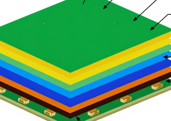
In multilayer PCBs, many inner-layer signal traces use a Stripline configuration, in which the signal conductor is located between two reference planes. Unlike a surface microstrip, the electrical environment of a stripline is determined by the dielectric layers and reference planes above and below the signal.
Because both dielectric layers contribute to the transmission-line structure, inner-layer impedance can be particularly sensitive to dielectric thickness, dielectric properties, copper geometry, and lamination variation. This makes stripline structures an important area of Impedance Control for high-speed multilayer PCB manufacturing.
A design may pass nominal impedance simulation but still experience significant impedance variation during mass production if the actual dielectric construction differs from the modeled stackup. Therefore, engineers need to consider material selection, dielectric symmetry, lamination behavior, copper distribution, simulation tolerances, and production verification as part of the complete design process.
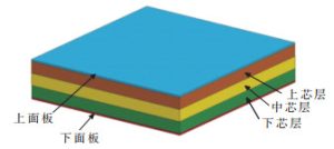
1. Stripline Impedance Model: The Importance of Dielectric Symmetry
A Stripline can generally be categorized as a symmetric or asymmetric structure.
In a symmetric stripline, the signal trace is positioned approximately midway between the upper and lower reference planes. The dielectric thickness above and below the trace is designed to be similar, creating a relatively balanced electromagnetic environment.
A simplified structure can be represented as:
Reference Plane → Dielectric → Signal Trace → Dielectric → Reference Plane
This configuration is often attractive for high-speed multilayer designs because the balanced geometry can make impedance modeling and manufacturing control more straightforward.
An asymmetric stripline has different dielectric thicknesses above and below the signal trace. It can still be designed and manufactured successfully, but the impedance calculation must accurately account for the actual geometry. The structure may also exhibit greater sensitivity to changes in one dielectric layer.
The goal should not be to assume that every stripline must be perfectly symmetrical. Instead, the design should ensure that the stackup model accurately represents the real manufactured structure and provides sufficient tolerance margin.
Use Compatible Dielectric Materials
Even when the dielectric thickness above and below a signal trace is similar, using different dielectric systems can produce different electrical behavior.
For example, combining a high-speed low-Dk material on one side of the trace with a conventional FR-4-based dielectric on the other side can result in an asymmetric electromagnetic environment.
The effective electrical properties of the transmission line will then depend on both materials.
For demanding impedance-controlled designs, it is generally preferable to use compatible dielectric systems above and below the stripline where the stackup permits. If different materials must be used, their actual electrical properties should be included in the Impedance Simulation model.
2. Dielectric Thickness Distribution in the PCB Stackup
The PCB Stackup should be established before detailed routing begins.
For example, a six-layer board may use a structure in which an inner signal layer is positioned between two reference planes. The dielectric spacing between the signal and each reference plane becomes an important part of the impedance calculation.
One common design mistake is to use the nominal thickness of a prepreg sheet directly as the final dielectric thickness in the impedance model.
Prepreg does not necessarily retain its original supplied thickness after lamination. During the multilayer lamination process, resin flows and fills the spaces around copper features. The final dielectric thickness depends on factors such as:
- Prepreg construction
- Resin content
- Glass style
- Copper thickness
- Copper distribution
- Lamination pressure
- Temperature profile
- Pressing conditions
- Finished stackup requirements
Therefore, impedance simulation should use an appropriate post-lamination dielectric thickness or a validated stackup model rather than simply copying the nominal incoming prepreg thickness.
3. Prepreg Selection and Resin Content
Prepreg (PP) is a critical component of multilayer dielectric construction.
Different glass styles and resin contents behave differently during lamination. A higher resin-content prepreg may provide greater resin flow and filling capability, while glass-rich constructions may behave differently under pressure and temperature.
However, it is not technically accurate to state that low-resin-content prepreg is always better for impedance control.
The appropriate prepreg construction depends on:
- Required dielectric thickness
- Copper pattern
- Resin filling requirements
- Glass style
- Lamination capability
- Electrical requirements
- Mechanical requirements
- Reliability requirements
For tightly controlled impedance, the key objective is predictable post-lamination dielectric geometry.
Engineers should therefore work with the PCB manufacturer to determine which prepreg construction can achieve the required finished dielectric thickness consistently.
4. Lamination Process and Its Effect on Inner-Layer Impedance
Lamination is one of the most important manufacturing processes affecting dielectric thickness.
During multilayer lamination, temperature and pressure control the flow and curing behavior of the resin system. Variations in the lamination profile can change the final thickness and distribution of the dielectric layers.
If prototype production and mass production use different process conditions, the resulting PCB stackup may also differ.
For example, a prototype may meet the target impedance while a volume-production lot exhibits impedance drift because of differences in:
- Pressing conditions
- Heating rate
- Curing profile
- Pressure control
- Material construction
- Copper distribution
- Panel configuration
For this reason, the PCB Stackup should be validated using a manufacturing process that can be transferred consistently into volume production.
During NPI, the material system, prepreg construction, stackup, and key lamination parameters should be reviewed and controlled before the design is released for mass production.
5. Copper Distribution and Dielectric Uniformity
Copper distribution can significantly affect resin flow during lamination.
Large copper areas and large copper-free regions can create different local resin-flow conditions. As a result, the final dielectric thickness may vary across different regions of the PCB.
This becomes particularly important for inner-layer Stripline structures because both the upper and lower dielectric layers contribute to the transmission-line geometry.
Designers should therefore review copper distribution during PCB layout and DFM analysis.
Recommended practices include:
- Maintaining reasonable copper balance between layers
- Avoiding unnecessarily large copper-free areas
- Reviewing large isolated copper regions
- Using copper balancing features when appropriate
- Maintaining continuous reference planes for high-speed signals
- Avoiding unnecessary openings in reference planes beneath impedance-controlled traces
The objective is not to make every layer geometrically identical, but to avoid extreme copper-density differences that may make lamination behavior less predictable.
6. Stripline Impedance Simulation Requirements
When simulating a Stripline, engineers should use a transmission-line model appropriate for the actual structure rather than applying a surface microstrip approximation.
The simulation should account for parameters such as:
- Upper dielectric thickness
- Lower dielectric thickness
- Upper dielectric Dk
- Lower dielectric Dk
- Copper thickness
- Trace width
- Trace spacing for differential pairs
- Reference-plane configuration
- Surface-finish and conductor effects where relevant
For a symmetric stripline, the upper and lower dielectric properties may be similar enough to simplify the model. For an asymmetric structure, both dielectric layers should be represented separately when the simulation tool supports this.
The model should also distinguish between nominal values and manufacturing tolerances.
7. Perform Worst-Case and Sensitivity Analysis
Nominal Impedance Simulation alone is not sufficient for a tightly controlled design.
Engineers should perform sensitivity analysis by varying the major manufacturing parameters within their expected tolerances.
Typical variables include:
- Upper dielectric thickness
- Lower dielectric thickness
- Dk
- Copper thickness
- Trace width
- Etching variation
- Layer registration
- Stackup variation
The analysis can then identify which parameters have the greatest influence on impedance.
For example, if the design is highly sensitive to dielectric thickness, tightening trace-width control alone may not significantly improve the final impedance distribution.
A practical design workflow is therefore:
Nominal Model → Sensitivity Analysis → Worst-Case Analysis → Stackup Optimization → Prototype Validation
If the predicted impedance range exceeds the product specification, engineers should modify the transmission-line geometry or material construction before production.
8. Differential Stripline Requires Additional Attention
Differential pairs routed as inner-layer striplines require control of more than just the single-ended impedance.
Engineers should consider:
- Differential impedance
- Pair spacing
- Trace width
- Trace-to-plane spacing
- Intra-pair length matching where required
- Reference-plane continuity
- Glass-weave effects
- Via transitions
- Local copper structures
A discontinuity in the reference plane can affect the return-current path and increase common-mode conversion or other signal-integrity problems.
For high-speed differential interfaces, the complete channel should therefore be evaluated rather than treating impedance as an isolated trace-width problem.
9. Impedance Test Structures Must Represent the Inner-Layer Stripline
Production Impedance Testing is essential for validating the actual fabricated structure.
However, the test coupon must represent the structure being controlled.
An inner-layer stripline should not be validated solely through a surface microstrip coupon because the two structures have different dielectric environments and electromagnetic characteristics.
A suitable stripline coupon should reproduce the relevant:
- Signal layer
- Upper and lower reference planes
- Dielectric construction
- Trace geometry
- Copper thickness
- Stackup relationship
The coupon should also be designed to work with the selected TDR measurement method.
10. Use TDR Testing to Verify Production Stability
Impedance Testing using Time-Domain Reflectometry (TDR) can be used to verify whether the fabricated transmission line meets its specified impedance range.
Before production, the manufacturer and customer should agree on:
- Test method
- Coupon structure
- Measurement locations
- Calibration requirements
- Target impedance
- Tolerance
- Sampling plan
- Acceptance criteria
For demanding multilayer PCBs, it can also be useful to analyze impedance results from different production locations to investigate possible regional variation.
If the measured impedance is consistently higher or lower than the simulated target, the engineering team should investigate the actual manufactured stackup rather than simply changing trace width.
Potential causes include:
- Actual dielectric thickness
- Dk variation
- Copper thickness
- Etching
- Lamination behavior
- Stackup construction
- Test-coupon design
- Measurement conditions
11. Prototype-to-Mass-Production Validation
One of the most important objectives of inner-layer impedance control is to achieve consistency between prototype and volume production.
During prototype manufacturing, engineers should compare:
- Designed stackup
- Simulated impedance
- Actual fabricated stackup
- Measured impedance
If the measured results differ significantly from the simulation, the model should be reviewed before production release.
The investigation should determine whether the discrepancy originates from material data, dielectric thickness, copper geometry, fabrication variation, or measurement methodology.
Once the root cause is understood, the validated stackup and process conditions can be carried forward into mass production.
12. Common Inner-Layer Stripline Design Mistakes
| Common Mistake | Potential Risk | Recommended Approach |
|---|---|---|
| Using microstrip calculations for stripline | Incorrect impedance model | Use an appropriate stripline model |
| Using PP nominal thickness directly | Simulation may not match finished PCB | Use validated post-lamination thickness |
| Ignoring upper/lower dielectric differences | Impedance calculation error | Model both dielectric layers when necessary |
| Mixing incompatible dielectric materials | Effective electrical properties become difficult to predict | Use compatible materials or model them separately |
| Ignoring copper distribution | Local dielectric variation | Review copper balance |
| Using only surface impedance coupons | Inner-layer impedance may not be represented | Use a matching stripline coupon |
| Simulating only nominal conditions | Insufficient manufacturing margin | Perform tolerance and sensitivity analysis |
| Changing trace width without investigating materials | Root cause may remain unresolved | Review stackup and material variation first |
| Prototype and mass production use different processes | Production impedance drift | Validate a transferable manufacturing process |
13. Practical DFM Checklist for Stripline Impedance Control
Before releasing a multilayer PCB for production, engineers can use the following checklist:
- Confirm the complete PCB Stackup.
- Verify upper and lower dielectric thicknesses.
- Confirm the selected Prepreg (PP) construction.
- Review core and prepreg material specifications.
- Verify relevant Dk and Df data.
- Check whether the upper and lower dielectric systems are compatible.
- Review copper distribution and reference-plane continuity.
- Perform nominal Impedance Simulation.
- Perform sensitivity and worst-case analysis.
- Confirm trace width and spacing tolerances.
- Review the impedance coupon structure.
- Define the Impedance Testing method.
- Validate the stackup during prototype production.
- Compare simulated and measured impedance.
- Lock the validated manufacturing stackup before mass production.
14. Kingda Support for Multilayer Stripline Design
Kingda can support multilayer PCB projects that require controlled-impedance design, stackup review, DFM evaluation, and manufacturing validation.
For inner-layer Stripline structures, the engineering review can focus on dielectric symmetry, PCB Stackup construction, Prepreg (PP) selection, copper distribution, impedance simulation, and production Impedance Testing.
By considering dielectric construction and manufacturing variation during the design stage, engineers can create greater impedance margin and reduce the risk of discovering inner-layer impedance problems after mass production begins.
Conclusion
Stable inner-layer impedance depends on much more than trace width. In a Stripline structure, the signal trace interacts with both the upper and lower dielectric layers and reference planes. As a result, dielectric thickness, Dk, material selection, copper distribution, and lamination conditions all influence the final impedance.
A reliable Impedance Control strategy should combine accurate PCB Stackup modeling, appropriate Prepreg (PP) selection, manufacturing-tolerance analysis, controlled lamination, and representative Impedance Testing.
By validating the complete dielectric structure from simulation through prototype and mass production, engineers can improve impedance consistency, reduce manufacturing rework, and establish a more robust foundation for high-speed multilayer PCB applications.