Rigid PCB Manufacturer
High-Quality Rigid PCBs at Competitive Prices
We provide reliable rigid PCB manufacturing solutions for prototypes, small-batch production, and volume manufacturing. Our capabilities cover standard and advanced rigid PCB technologies for demanding electronic applications. Learn more about our complete PCB manufacturing services.
- 1–40 layers for production and up to 100 layers for prototypes
- FR-4, high-speed, microwave and RF, metal core, ceramic, and PTFE materials
- Blind and buried vias, stacked and staggered vias, and any-layer HDI
- Conductive and non-conductive via filling
- Back drilling, backplanes, embedded components, and IC substrates
- Custom PCB manufacturing for demanding electronic applications
-
High-Speed PCB
From household appliances and automotive electronics to industrial equipment and communication systems, rigid PCBs remain one of the most widely used circuit board technologies. Their mechanical strength, dimensional stability, and ability to support high-density multilayer designs make them suitable for a wide range of electronic products.
Get a Free Quote for Your Rigid PCB
Send us your PCB specifications, Gerber files, drawings, or other technical requirements. Our engineering team can review your project and provide a suitable manufacturing solution and quotation.
- Name
- Email Address
- Phone Number
- Project Details
What Is a Rigid PCB?
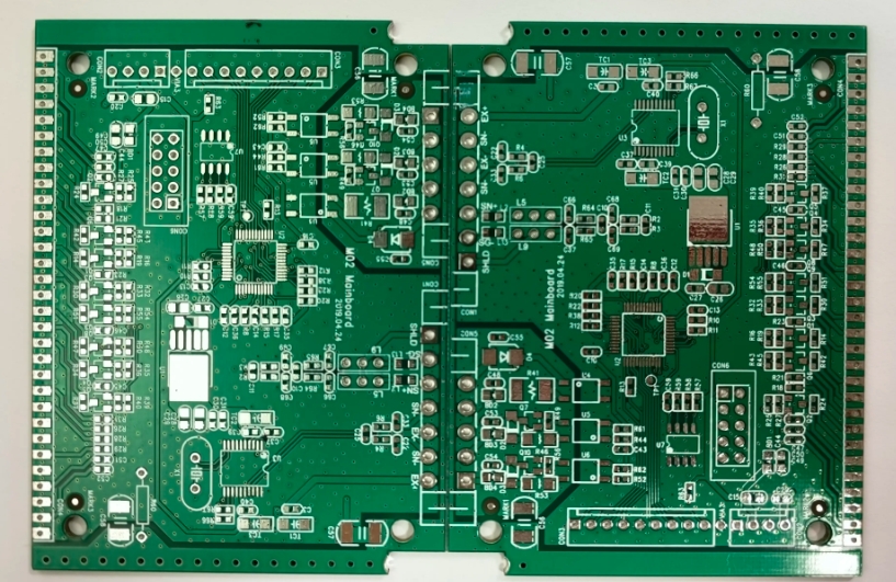
A rigid PCB is a printed circuit board manufactured on a solid substrate that maintains its shape during normal use. Unlike flexible PCBs, rigid circuit boards are not designed to bend or fold after manufacturing.
Rigid PCBs are widely used in automotive electronics, industrial equipment, consumer electronics, medical devices, telecommunications, and many other applications.
FR-4 is one of the most commonly used rigid PCB substrate materials. It consists of woven glass fiber reinforced with epoxy resin and provides a combination of mechanical strength, electrical insulation, thermal stability, and cost efficiency.
Depending on the application, other substrate materials may be selected to meet specific electrical, thermal, or mechanical requirements. These can include high-TG materials, PTFE-based materials, ceramic substrates, metal-core materials, and other high-performance laminates.
A typical rigid PCB consists of several functional layers, including:
- Substrate: Provides mechanical support and electrical insulation.
- Copper Layer: Forms the conductive paths and electrical connections.
- Solder Mask: Protects exposed copper and helps prevent solder bridges.
- Surface Finish: Protects exposed copper pads and improves solderability.
- Silkscreen: Provides component references, markings, logos, and other identification information.
Rigid PCBs can also be classified by their layer structure, including single-sided, double-sided, and multilayer PCBs. As the number of layers increases, the circuit board can accommodate more complex routing and higher component density.
What Are the Advantages of Rigid PCBs?
Rigid PCBs remain the preferred choice for many electronic products because of their mechanical stability, reliability, manufacturing maturity, and ability to support complex circuit designs.
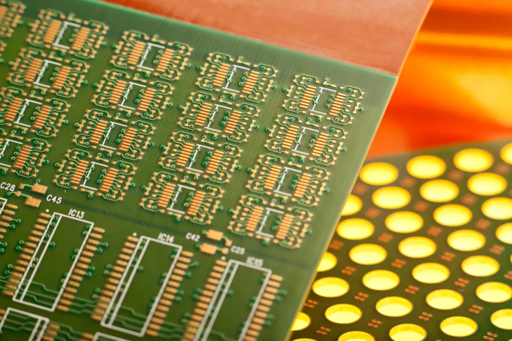
Higher Functional Density
Multilayer rigid PCBs allow designers to integrate multiple signal, power, and ground layers into a compact board structure.
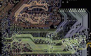
This makes rigid PCBs suitable for products requiring high circuit density, controlled impedance, high-speed signal transmission, and complex electrical connections.
Excellent Mechanical Strength
The rigid substrate provides strong mechanical support for electronic components and connectors.
Compared with flexible PCBs, rigid circuit boards maintain their shape and are less susceptible to mechanical deformation during installation and normal operation.
Efficient Manufacturing
Rigid PCB manufacturing is based on highly standardized and automated processes. Mature manufacturing technologies allow manufacturers to produce consistent circuit boards across prototypes, low-volume production, and mass production.
High Reliability
The solid construction of a rigid PCB provides good dimensional stability and mechanical durability.
When the appropriate materials, layer structure, copper thickness, surface finish, and manufacturing processes are selected, rigid PCBs can provide reliable long-term performance in demanding applications.
Flexible Design Options
Rigid PCB technology supports a wide range of configurations, including single-sided, double-sided, multilayer, HDI, high-frequency, metal-core, and other specialized PCB structures.
This allows engineers to select a board construction according to electrical, thermal, mechanical, and environmental requirements.
Rigid PCB Applications
Rigid circuit boards are used across a wide range of industries and electronic products.
Common applications include:
- Computer motherboards
- Storage and networking equipment
- Communication systems
- Wireless and RF equipment
- Automotive electronics
- Vehicle infotainment systems
- Medical equipment
- Industrial control systems
- Test and measurement equipment
- Consumer electronics
- Power electronics
- Smart home devices
- Telecommunications equipment
For applications requiring advanced signal integrity, thermal management, or high circuit density, specialized rigid PCB technologies can be combined with appropriate materials and manufacturing processes.
How Are Rigid PCBs Manufactured?
Rigid PCB manufacturing involves multiple controlled processes. Each stage contributes to the electrical performance, mechanical reliability, and overall quality of the finished circuit board.
Schematic and PCB Layout
The manufacturing process begins with the electronic design.
The schematic defines the electrical connections between components, while the PCB layout determines the physical placement of components, routing of traces, layer structure, vias, copper areas, and other board features.
Before production, the design should be reviewed for manufacturability, electrical performance, material requirements, and production constraints.
Lamination
For multilayer rigid PCBs, individual circuit layers are stacked together with dielectric materials such as prepreg.
The stack-up is subjected to controlled heat and pressure so that the resin flows and cures, bonding the individual layers into a solid multilayer structure.
Proper control of temperature, pressure, resin flow, and lamination time is essential for maintaining layer alignment and board reliability.
Photoresist Application
A photoresist layer is applied to the copper surface to define the circuit pattern.
The resist is selectively exposed to ultraviolet light according to the circuit image. During development, specific areas of the resist are removed, exposing the copper areas that will be processed during subsequent etching.
Copper Etching
Unwanted copper is removed using a controlled chemical etching process, leaving the required circuit traces and copper features.
Etching parameters must be carefully controlled to maintain trace width, spacing, and overall dimensional accuracy.
After etching, the board is cleaned to remove residual chemicals and photoresist materials.
Drilling
Mechanical drilling or laser drilling is used to create through-holes, vias, and other required openings.
High-density PCB designs may require microvias, blind vias, buried vias, or other advanced interconnection structures.
Drilling parameters such as spindle speed, feed rate, tool geometry, and hole diameter must be carefully controlled to achieve consistent results.
Solder Mask
A solder mask is applied over the PCB surface to protect copper traces and reduce the risk of solder bridges during assembly.
Liquid photoimageable solder mask is commonly used for high-density PCB manufacturing because it can provide accurate openings around component pads and other exposed copper areas.
Surface Finish
Exposed copper pads require an appropriate surface finish to protect the copper from oxidation and maintain good solderability.
Common surface finishes include:
- HASL
- Lead-free HASL
- ENIG
- OSP
- Immersion tin
- Immersion silver
The appropriate finish depends on factors such as component requirements, soldering process, product life cycle, environmental requirements, and cost.
Silkscreen
Silkscreen is used to add identification and assembly information to the PCB surface.
Typical markings include:
- Component reference designators
- Pin indicators
- Polarity markings
- Company logos
- Product identification
- Regulatory markings
- Traceability information
For high-density boards, accurate silkscreen positioning is important to ensure clear identification without interfering with component pads or other critical features.
Why Choose a Professional Rigid PCB Manufacturer?
Selecting the right rigid PCB manufacturer can directly affect product quality, development time, manufacturing cost, and production reliability.
Broad Manufacturing Capabilities
Rigid PCB requirements vary significantly depending on the application. A reliable manufacturer should be able to support different layer counts, materials, copper weights, surface finishes, via structures, and PCB technologies.
From conventional FR-4 boards to advanced multilayer, HDI, high-frequency, and specialized rigid PCB designs, manufacturing flexibility is essential for supporting different engineering requirements.
Engineering Support
Professional engineering support helps identify potential manufacturing issues before production begins.
Design review, DFM analysis, stack-up evaluation, material selection, and manufacturing documentation review can help reduce production risks and avoid unnecessary redesigns.
Competitive Manufacturing Costs
PCB cost depends on multiple factors, including board size, layer count, material, copper thickness, quantity, surface finish, via technology, and manufacturing complexity.
An experienced manufacturer can evaluate the complete design and recommend an appropriate manufacturing approach based on performance and cost requirements.
Consistent Quality Control
Reliable PCB manufacturing requires quality control throughout the entire production process.
Inspection and process control can help verify materials, dimensions, copper structures, solder mask quality, surface finish, electrical performance, and other critical specifications.
Fast and Reliable Delivery
Efficient engineering review, material preparation, production scheduling, inspection, and logistics coordination can help shorten lead times while maintaining manufacturing consistency.
For prototype and production projects with strict schedules, responsive communication and accurate production planning are particularly important.
Frequently Asked Questions About Rigid PCBs
What materials are commonly used to manufacture rigid PCBs?
FR-4 is one of the most widely used materials for rigid PCBs. Depending on the application, manufacturers may also use high-TG laminates, PTFE materials, ceramic substrates, metal-core materials, and other specialized laminates.
What manufacturing technologies are used for rigid PCBs?
Common technologies include multilayer lamination, mechanical drilling, laser drilling, copper plating, photo imaging, etching, solder mask application, surface finishing, and electrical testing.
Advanced boards may additionally require HDI structures, microvias, blind and buried vias, via filling, back drilling, and controlled impedance manufacturing.
What tests are required for rigid PCBs?
Testing requirements depend on the PCB design and application. Typical inspection and testing methods may include visual inspection, automated optical inspection, dimensional inspection, electrical testing, X-ray inspection, and other customer-specific tests.
How long does it take to manufacture a rigid PCB?
Lead time depends on factors such as layer count, material, board complexity, quantity, surface finish, via structure, and testing requirements.
Prototype boards generally require a shorter production cycle than complex multilayer or high-volume production orders.
What is the difference between rigid and flexible PCBs?
Rigid PCBs use a solid substrate and maintain their shape during normal operation. Flexible PCBs use flexible materials that allow the circuit to bend or fold.
Rigid PCBs are generally preferred when mechanical stability and structural support are important, while flexible PCBs are advantageous when space constraints or dynamic bending are major design considerations.
How much does a rigid PCB cost?
The cost of a rigid PCB depends on board dimensions, layer count, material, copper thickness, quantity, surface finish, hole technology, manufacturing tolerances, and other technical requirements.
Providing complete Gerber files, PCB specifications, and quantity requirements allows the manufacturer to provide a more accurate quotation.
What are the main benefits of rigid PCBs?
The major benefits include high mechanical strength, dimensional stability, reliable electrical performance, mature manufacturing processes, high-density multilayer capability, and broad material and technology options.
Are there disadvantages to rigid PCBs?
Rigid PCBs cannot normally be bent after manufacturing and require a fixed installation space. For products with severe space limitations or dynamic movement, flexible or rigid-flex PCBs may be more suitable.
Are rigid PCBs cost-effective compared with other PCB types?
For many conventional electronic products, rigid PCBs offer an excellent balance between manufacturing cost, reliability, mechanical strength, and electrical performance.
The most cost-effective solution depends on the specific application and technical requirements.
What is the difference between rigid PCB and rigid-flex PCB?
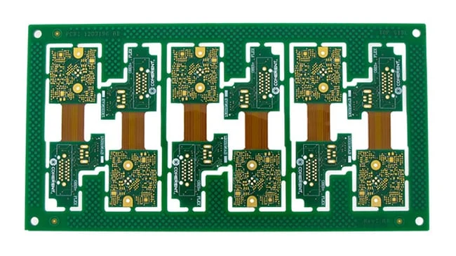
A rigid PCB uses rigid substrates throughout the board, while a rigid-flex PCB combines rigid sections with flexible circuit sections.
Rigid-flex technology is useful when a product requires both structural support and flexible electrical connections within a compact assembly.
What is the difference between rigid PCB and semi-rigid PCB?
A rigid PCB is designed to remain mechanically rigid, while a semi-rigid PCB uses specialized materials or structures that provide limited flexibility.
The appropriate solution depends on the required mechanical movement, installation conditions, electrical requirements, and product design.
Reliable Rigid PCB Manufacturing for Your Project
Choosing a capable manufacturing partner is essential when your project requires reliable rigid PCBs, consistent quality, engineering support, and scalable production. From standard FR-4 boards to complex multilayer, HDI, high-frequency, and specialized rigid PCB designs, the manufacturing process should be matched carefully to your technical requirements.
With integrated PCB manufacturing, PCB assembly, component sourcing, testing, and engineering support, GOPCBA provides a streamlined manufacturing solution from PCB fabrication through finished electronic assemblies. For your next rigid PCB project, contact our team for a quotation and send us your Gerber files, specifications, BOM, or project requirements.