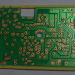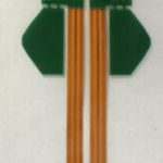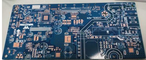
Multilayer PCB manufacturing is an important part of modern electronics production. As electronic products become smaller, faster, and more highly integrated, multilayer PCBs are increasingly used to accommodate complex circuits within limited board space.
Kingda provides professional PCB manufacturing solutions covering multilayer PCBs, high-density interconnect (HDI) PCBs, thick copper boards, precision double-sided PCBs, impedance-controlled PCBs, flexible PCBs, and other advanced circuit board technologies.
Multilayer PCBs are widely used in computers, medical equipment, automotive electronics, communication systems, industrial controls, consumer electronics, aerospace, and other high-performance applications.
What Is a Multilayer PCB?
A multilayer PCB consists of three or more conductive copper layers separated by insulating dielectric materials. The different conductive layers are interconnected through vias, allowing designers to achieve higher circuit density and more complex routing within a relatively compact board.
Compared with single-sided and double-sided PCBs, multilayer boards offer several advantages:
- Higher circuit density
- More compact product designs
- Better signal integrity
- Improved power distribution
- Greater routing flexibility
- Better electromagnetic compatibility
- Support for complex high-speed circuits
Multilayer construction is particularly suitable for products that require high functionality in a limited physical space.
Blind Vias and Buried Vias
Vias are essential components of multilayer PCB manufacturing because they provide electrical connections between different conductive layers.
There are several common types of vias, including through vias, blind vias, and buried vias.
Blind vias connect an outer surface layer to one or more inner layers without passing through the entire PCB. Because they do not extend through the complete board, blind vias can save routing space and support higher circuit density.
Buried vias connect two or more inner layers but do not extend to the outer surface of the finished PCB. As a result, they are completely enclosed within the multilayer structure.
Both blind and buried vias are frequently used in high-density and HDI PCB designs.
Why Blind and Buried Vias Matter
As PCB dimensions become smaller and component density increases, conventional through-hole vias can consume valuable routing space.
Blind and buried vias provide greater flexibility for interlayer connections.
Their main advantages include:
- Improved routing density
- More efficient use of PCB space
- Reduced interference with surface components
- Support for fine-pitch components
- Greater flexibility in multilayer stack-up design
- Improved suitability for HDI applications
However, blind and buried vias also increase manufacturing complexity. Their design must therefore take into account drilling technology, layer structure, aspect ratio, registration accuracy, plating reliability, and manufacturing tolerances.
PCB Hole Size and Aspect Ratio
The minimum finished hole diameter is closely related to the overall thickness of the PCB.
A key manufacturing parameter is the hole aspect ratio, which is generally defined as the ratio between the hole depth and the finished hole diameter.
As the board becomes thicker, a smaller hole diameter becomes increasingly difficult to drill and plate reliably.
For conventional mechanical drilling, the designer should therefore consider the relationship between:
- Board thickness
- Finished hole diameter
- Drill diameter
- Copper plating thickness
- Hole aspect ratio
- Drilling accuracy
Typical aperture sizes may include 24 mil, 20 mil, 16 mil, 12 mil, and 8 mil, depending on the PCB structure and manufacturing process.
These values should be treated as design references rather than universal manufacturing limits because the actual minimum hole size depends on the PCB manufacturer’s equipment and process capability.
Pad Size and Via Design
The diameter of the pad surrounding a via must provide sufficient clearance for drilling and plating while maintaining reliable electrical and mechanical connections.
Typical pad dimensions may vary according to the hole diameter and PCB fabrication process.
For example, larger holes generally require larger pads, while advanced HDI structures can use smaller microvias and optimized pad geometries.
When designing vias, engineers should consider:
- Finished hole diameter
- Pad diameter
- Annular ring
- Copper thickness
- Via-to-via spacing
- Via-to-trace clearance
- Via-to-pad clearance
- Board thickness
- Manufacturing tolerance
For high-density designs, excessively large pads can reduce available routing space, while insufficient annular rings can increase the risk of manufacturing defects.
Therefore, via dimensions should always be developed according to the capabilities of the selected PCB manufacturer.
Test Holes for PCB Testing
Test holes are conductive holes or vias designed to facilitate electrical testing during PCB production.
They can be used for ICT (In-Circuit Test), fixture-based testing, probing, and other electrical verification processes.
Test points should be positioned to provide sufficient accessibility for testing equipment.
Important considerations include:
- Test pad diameter
- Distance between test points
- Probe accessibility
- Component clearance
- Test fixture requirements
- Electrical connectivity
A commonly used design reference is a test pad diameter of approximately 25 mil or larger, although actual requirements depend on the selected testing method and equipment.
Adequate spacing between test points is also necessary to prevent probe interference and ensure reliable testing.
Trace Width and Trace Spacing
PCB trace width and PCB trace spacing are two fundamental parameters in multilayer PCB design.
The appropriate trace width depends on several factors, including current carrying capacity, copper thickness, allowable temperature rise, signal frequency, impedance requirements, and manufacturing capability.
For power or high-current circuits, wider traces may be required to reduce resistance and heat generation.
For high-density signal routing, narrower traces can increase routing flexibility, but excessively narrow traces may increase manufacturing difficulty and reduce reliability.
PCB trace spacing must also provide sufficient electrical isolation between adjacent conductors.
The required spacing depends on:
- Operating voltage
- Signal characteristics
- Crosstalk requirements
- Impedance control
- PCB manufacturing capability
- Safety and creepage requirements
Therefore, trace width and spacing should not be determined solely by board density.
Factors Affecting Trace Width and Spacing
1. PCB Routing Density
The overall circuit density has a major influence on routing requirements.
When component density and connection complexity increase, designers may need narrower traces and smaller spacing to complete all required connections.
This is particularly common in HDI PCB designs and compact electronic products.
However, reducing trace width and spacing beyond the manufacturer’s proven capability can increase production costs and reduce manufacturing yield.
2. Signal Current
Current carrying capacity is another important consideration.
A trace carrying a higher current generally requires a wider conductor or greater copper thickness.
If the trace is too narrow, resistive losses and temperature rise can increase.
Therefore, PCB designers should calculate the appropriate trace width based on current requirements rather than selecting a minimum width simply to save space.
3. Signal Frequency and Impedance
For high-speed signals, trace width and spacing also affect transmission characteristics.
Controlled-impedance traces require careful coordination among:
- Trace width
- Copper thickness
- Dielectric thickness
- Dielectric constant
- Reference-plane distance
- PCB stack-up
This is especially important for high-speed interfaces, RF circuits, communication equipment, and other applications where signal integrity is critical.
Multilayer PCB Stack-Up Considerations
A well-designed multilayer PCB stack-up is essential for electrical performance and manufacturability.
A typical multilayer structure may contain:
- Signal layers
- Ground planes
- Power planes
- Prepreg dielectric layers
- Core materials
- Copper foil
Ground and power planes can provide low-impedance return paths and help reduce electromagnetic interference.
For high-speed circuits, signal layers should be arranged with appropriate reference planes to maintain controlled impedance and minimize unwanted coupling.
Stack-up design should also consider PCB thickness, material selection, copper weight, dielectric thickness, thermal requirements, and fabrication processes.
HDI PCB and Advanced Interconnection Technology
HDI PCB technology takes multilayer interconnection one step further by using microvias, fine lines, fine spaces, and sequential build-up structures.
Microvias are typically formed using laser drilling and can connect adjacent layers with very small diameters.
HDI technology enables designers to:
- Reduce PCB size
- Increase wiring density
- Support fine-pitch components
- Improve routing efficiency
- Reduce via size
- Create more compact electronic products
However, HDI manufacturing requires high registration accuracy, precise laser drilling, reliable copper plating, and strict process control.
PCB Manufacturing Capabilities Matter
The same PCB design may be manufactured successfully by one supplier but become difficult or uneconomical for another supplier.
This is because manufacturing capability depends on equipment, process control, engineering experience, material systems, inspection technology, and production management.
Before finalizing a PCB design, designers should communicate with the manufacturer regarding:
- Minimum trace width
- Minimum trace spacing
- Minimum finished hole diameter
- Minimum annular ring
- Blind and buried via capability
- Maximum board thickness
- Copper thickness
- Layer count
- Impedance-control capability
- HDI process capability
Working with the manufacturer during the design stage can reduce redesigns, manufacturing risks, and unnecessary production costs.
Conclusion
Modern electronic products require increasingly compact and sophisticated circuit architectures. Multilayer PCB manufacturing provides an effective solution by increasing routing density while maintaining the electrical and mechanical performance required by advanced electronic systems.
The correct design of blind vias, buried vias, hole sizes, pads, PCB trace width, and PCB trace spacing is essential for achieving reliable multilayer PCB performance.
For high-density applications, HDI PCB technology provides additional routing flexibility through microvias and sequential build-up structures. At the same time, successful PCB production depends on selecting appropriate materials, designing a manufacturable stack-up, and matching the design with the manufacturer’s actual process capabilities.
With professional engineering support and controlled manufacturing processes, Kingda can provide multilayer PCB solutions for high-density, high-speed, automotive, medical, communication, industrial, and other advanced electronic applications.