When designing RF and microwave systems, engineers pay close attention to intermodulation distortion (IMD), especially in applications where multiple high-power signals are transmitted simultaneously. In passive circuits such as antennas, transmission lines, cables, connectors, filters, and other RF components, a related phenomenon known as Passive Intermodulation (PIM) can become a significant source of interference.
PIM occurs when nonlinear behavior exists in an otherwise passive RF structure. When two or more signals are transmitted through a nonlinear passive circuit, their frequency components can mix and generate unwanted intermodulation products. If these products fall within or near a receiver’s operating band, they can interfere with weak received signals and reduce overall system sensitivity.
For this reason, controlling PIM Performance is an important consideration in High-Frequency PCB design, particularly for wireless base stations, antennas, RF front ends, filters, and other communication equipment.
What Is Passive Intermodulation (PIM)?
In an ideal linear circuit, signals pass through the system without generating new frequency components. However, real-world passive structures can exhibit a small degree of nonlinear behavior.
Assume two input signals have frequencies of f1 and f2. Nonlinear interactions can generate intermodulation products such as:
- 2f1 − f2
- 2f2 − f1
- 3f1 − 2f2
- 3f2 − 2f1
- Other higher-order mixing products
Third-order products are particularly important in many RF systems because they can fall close to the desired receive frequency.
For example, if a transmitter operates at relatively high power while a receiver operates nearby in frequency, a third-order PIM product generated by the transmitter path may fall directly into the receiver’s frequency band.
Because the unwanted signal may be much weaker than the original transmit signal, it can be difficult to detect during normal operation. Nevertheless, even a relatively low-level PIM product can degrade receiver sensitivity when the desired signal is extremely weak.
Why Is PIM Important in High-Frequency PCB Design?
The amplitude of PIM products is influenced by several factors, including:
- Input signal power
- Signal frequency
- Number of simultaneously transmitted signals
- Circuit geometry
- Current density
- Surface condition of conductors
- Mechanical contacts
- Material properties
- Manufacturing quality
As transmit power increases, the potential impact of nonlinearities becomes more significant. At the same time, higher signal density and wider operating bandwidths make it increasingly important to control unwanted intermodulation products.
Therefore, low-PIM design cannot depend on PCB material selection alone. The complete RF structure—including conductor geometry, interfaces, connectors, vias, solder joints, and mechanical contacts—must be considered.
The Influence of Metal Contacts on PIM
One of the most common causes of PIM in passive RF systems is poor metal-to-metal contact.
In communication equipment, RF connectors, antenna interfaces, cable connections, and other mechanical interfaces may develop nonlinear behavior when the contact surface is contaminated, oxidized, mechanically damaged, or insufficiently tightened.
For example, a contaminated or imperfect metal interface can create a microscopic nonlinear contact. When high RF current flows through this area, the nonlinear contact can generate intermodulation products.
Potential causes include:
- Oxidation on metal surfaces
- Dirt or foreign particles
- Poor mechanical contact
- Insufficient contact pressure
- Surface contamination
- Damaged plating
- Loose connectors
- High local current density
This is why low-PIM design must address not only the PCB itself but also connectors, fasteners, shielding structures, cables, and other conductive interfaces.
Copper Roughness and PIM Performance
The conductor surface of a PCB can also influence RF performance.
In High-Frequency PCB applications, copper roughness is commonly discussed because it affects conductor loss, signal propagation, and high-frequency electrical behavior. For low-PIM applications, conductor surface characteristics may also influence the quality and consistency of RF current distribution.
A smoother copper surface can provide more predictable RF behavior and reduce certain sources of localized current concentration.
However, copper roughness should not be treated as the only factor determining PIM Performance. PIM is generally a system-level characteristic affected by circuit geometry, interfaces, assembly quality, current density, and mechanical construction.
Therefore, PCB designers should evaluate copper surface characteristics together with the complete RF structure rather than selecting a material based on one parameter alone.
PCB Material Selection for Low-PIM Applications
Selecting the appropriate PCB Material is important for RF and microwave circuits.
High-frequency laminates are typically selected according to parameters such as:
- Dielectric constant (Dk)
- Dissipation factor (Df)
- Thermal stability
- Dimensional stability
- Copper surface characteristics
- Frequency-dependent electrical performance
- Manufacturing compatibility
Low-loss materials can help reduce insertion loss and maintain predictable RF performance. However, low dielectric loss does not automatically mean low PIM.
This distinction is important.
A PCB laminate may provide excellent dielectric performance while the completed circuit still exhibits undesirable PIM because of poor conductor geometry, high current density, mechanical interfaces, solder joints, or contamination.
Consequently, PCB Design and manufacturing quality are just as important as material selection.
Current Density and PIM
Current density is another important factor affecting PIM.
When RF current is concentrated in a small area, localized electrical stress can increase. Complex circuit structures, narrow transmission-line sections, sharp geometry transitions, and coupling structures may produce different current distributions even when they are manufactured from the same PCB material.
Consider three different RF structures fabricated using the same laminate:
- A simple microstrip transmission line
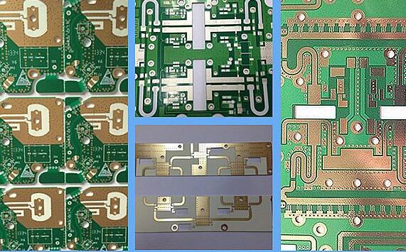
- An edge-coupled bandpass filter
- A stepped-impedance low-pass filter
Although the three structures use the same material, their current distributions can be significantly different.
A simple transmission line generally has a relatively uniform current distribution. A coupled filter, by contrast, may have areas where electromagnetic coupling and current concentration are more pronounced.
As a result, the three circuits can exhibit substantially different PIM Performance even though their substrate material is identical.
This demonstrates an important principle: PIM is not simply a property of the laminate. The electrical and mechanical structure of the completed circuit has a major influence.
Circuit Geometry and RF Linearity
A well-designed RF circuit should maintain a highly linear signal path under the intended operating conditions.
Circuit geometry can affect:
- Current distribution
- Electric-field concentration
- Impedance continuity
- RF coupling
- Conductor losses
- Local heating
- Mechanical contact behavior
Abrupt geometry changes, unnecessary discontinuities, poorly controlled interfaces, and areas of excessive current concentration should therefore be carefully evaluated during PCB Design.
For low-PIM applications, designers should pay particular attention to transmission-line transitions, connector launches, vias, grounding structures, filter coupling sections, and other areas where RF current may become concentrated.
Manufacturing Quality and PIM
Even a well-designed RF PCB can exhibit poor PIM if manufacturing quality is inconsistent.
Important manufacturing considerations include:
Copper and Surface Quality
Copper surfaces should be clean and properly processed. Excessive contamination, oxidation, or inconsistent surface treatment can affect RF interfaces and electrical performance.
Plating Quality
Plated through-holes, vias, pads, and connector interfaces should have consistent plating quality. Poor plating or mechanical damage may create undesirable electrical discontinuities.
Soldering Quality
Solder joints in RF current paths should be properly formed and controlled. Voids, cracks, insufficient solder, or inconsistent solder geometry can affect electrical continuity and reliability.
Mechanical Assembly
Connectors and other conductive interfaces should have consistent mechanical contact. Improper assembly torque, contamination, or damaged contact surfaces can increase the risk of PIM.
Cleanliness
Manufacturing residues and foreign materials should be controlled carefully, especially in high-power RF applications.
Therefore, low-PIM manufacturing requires cooperation between PCB design, material selection, fabrication, assembly, and final inspection.

How to Reduce PIM in High-Frequency PCB Applications
A comprehensive low-PIM strategy should include the following measures:
- Select an appropriate PCB Material for the operating frequency and power level.
- Control copper surface characteristics and avoid unnecessary conductor roughness.
- Optimize transmission-line geometry to maintain consistent current distribution.
- Reduce areas of excessive current density.
- Minimize unnecessary discontinuities in RF signal paths.
- Carefully design connectors, vias, transitions, and grounding structures.
- Maintain clean and reliable metal-to-metal interfaces.
- Control soldering and plating quality.
- Prevent contamination and oxidation of conductive surfaces.
- Verify PIM Performance through appropriate RF testing.
The exact requirements depend on the operating frequency, transmit power, bandwidth, circuit structure, and application environment.
PIM Testing and Evaluation
PIM testing is normally performed by transmitting two or more RF tones at specified power levels and measuring the resulting intermodulation products.
PIM is commonly expressed in dBc, which represents the unwanted intermodulation signal relative to the carrier power.
A lower PIM level generally indicates better linearity and lower interference.
However, test results should always be interpreted together with the test conditions. Different frequencies, transmit power levels, fixtures, connectors, cable assemblies, and measurement configurations can produce different results.
Therefore, when comparing materials or PCB structures, the testing conditions must be controlled consistently.
Kingda’s Approach to Low-PIM RF PCB Manufacturing
For demanding High-Frequency PCB applications, Kingda emphasizes the relationship between material selection, circuit design, manufacturing precision, and assembly quality.
A low-PIM RF circuit cannot be achieved simply by choosing a low-loss laminate. The entire signal path must be considered, from PCB material and copper structures to vias, connectors, solder joints, and mechanical interfaces.
Kingda can support RF PCB projects by focusing on:
- High-frequency PCB fabrication
- Controlled impedance requirements
- High-quality copper processing
- Precision drilling and plating
- RF transmission-line structures
- Multilayer RF PCB manufacturing
- Manufacturing process control
- Inspection and electrical testing
By integrating PCB Design considerations with manufacturing process control, designers can achieve more predictable RF performance and reduce potential sources of passive intermodulation.
Conclusion
Passive Intermodulation (PIM) is an important consideration in modern RF and microwave systems, particularly where high-power transmit signals operate close to sensitive receiver bands.
PIM can be influenced by metal-to-metal contacts, contamination, mechanical interfaces, current density, circuit geometry, copper surface characteristics, manufacturing quality, and material selection.
Although PCB Material plays an important role in RF performance, PIM should not be considered an inherent property of the material alone. The complete circuit structure and manufacturing process can have an equally important impact.
For this reason, successful low-PIM High-Frequency PCB development requires a combination of appropriate materials, optimized PCB Design, controlled current distribution, reliable conductive interfaces, and consistent manufacturing quality.
For RF communication, antenna, filter, and other high-frequency applications, Kingda can help customers evaluate PCB manufacturing requirements and develop reliable solutions with controlled RF performance.