PCB Electrical Test Methods: Flying Probe and Grid
A finished board that leaves the shop with an undetected open circuit does not simply get scrapped. It travels to the assembly line, collects components, passes through reflow and possibly through in-circuit test, and only then reveals the defect, at which point the assembler bills the board shop for components, rework and inspection. PCB electrical test exists to catch that defect while it is still a bare board and the only remedy is a short jumper. This article compares the main methods, the stages at which they are applied, and the design decisions that decide how well they work.
Why bare board testing exists
Short circuits, open circuits and leakage appear during the many wet and thermal steps of fabrication even on a controlled line. As density rises and spacing narrows, the probability that a defect escapes an intermediate stage rises with it, and the cost of finding it rises far faster. The widely used rule of ten describes the pattern: the cost of correcting a fault grows by roughly an order of magnitude at each stage of assembly. Finding an open on the bare board costs a repair, a jumper or at worst one panel. Finding the same open after the customer has populated the board costs the components, the labour and the inspection. Finding it in a finished system costs orders of magnitude more.
The three test stages
Testing is applied at three points in the fabrication flow: after inner-layer etching, after outer-layer etching, and on the finished board. Each stage typically runs a full 100 percent test, with two or three passes in total across the build. The data is as valuable as the screening itself. Yields by defect type, tracked across stages, point directly at the process step that is drifting, and re-testing after rework closes the loop by confirming the repair.
What the test specification must define
Before the first panel is probed, the fabricator and the customer agree on the test conditions. Five items matter: the source and format of the test data, the electrical conditions such as voltage, current, continuity and insulation resistance thresholds, how the fixture will be built and which points will be selected, the test stamp or marking applied to a passing board, and the repair specification that says what rework is acceptable. Ambiguity in any of these produces arguments at shipment rather than at design review. It is also worth agreeing in advance on which nets are excluded and why, because an exclusion that is never documented becomes a coverage gap that nobody can audit later.
Dedicated fixture testing
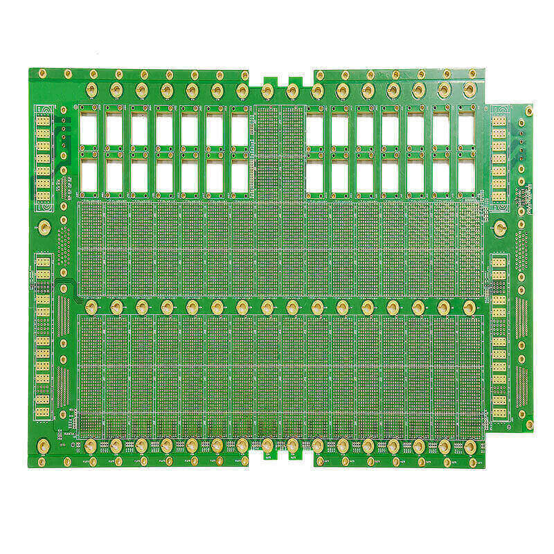
A dedicated test fixture is built for one part number and cannot be reused for another, which makes it a capital cost that must be amortised over the order. The fixture holds a bed of probes matching the pad locations, and the panel is pressed onto it so all nets are checked at once. A single-sided fixture handles up to about 10,240 test points, and a double-sided fixture around 8,192 points per side. Because probe diameter limits how closely probes can be packed, dedicated fixtures suit designs with moderate pitch. For high-volume production of a stable design they are the fastest option per board, and the fixture cost disappears against the volume.
Universal grid testing and ATE
A universal grid test takes advantage of the fact that most board layouts are based on a regular grid. A mask made from a rigid base material is drilled only where the grid intersects a net, so only those locations allow a probe through. One standard grid fixture can then serve many part numbers by swapping the mask and the moving probe set, which makes fixture preparation fast and the probes reusable. Point counts above 10,000 are normal, and the machine can apply a higher voltage, commonly 250 V, to verify insulation as well as continuity. In that configuration the universal grid tester is often called automatic test equipment. Layouts that stay on the grid are known as on-grid and test easily; fine-pitch designs that leave the grid require off-grid testing and a specially designed fixture.
Flying probe test
A flying probe test needs no fixture at all. Two moving probes step through the coordinates in x, y and z and check each net end to end, which removes the fixture cost and the lead time entirely. The trade-off is speed: the probes move one point at a time, so throughput is roughly 10 to 40 points per second, making the method far slower than a bed-of-nails fixture. That makes flying probe test ideal for prototypes, samples and small batches, and for very high-density boards where a fixture could not be built within the pitch. It is the usual choice when the multilayer prototype requirements call for a verified first article before production tooling is ordered. For a new design with no production history, it is usually the fastest way to get a verified board in hand.
Designing for testability
The test method should be chosen before the layout is frozen, because each method imposes different constraints on pad size, spacing and access. A board intended for a dedicated fixture needs test points that a probe can reach on both sides. A board intended for a universal grid needs its critical nets on the grid. A board intended for flying probe can use very fine pitch but will need generous test-point access so the probes do not have to land on a component pad, where a probe mark could affect soldering. Reserve test pads on the bottom side, keep them away from tall components, and label them consistently with the netlist. The quality characteristics of a PCB design include testability for exactly this reason.
Cost follows directly from the choice. A dedicated fixture makes sense when volume is high and the design is stable; a universal grid machine is efficient for a mix of high-volume part numbers at moderate density; flying probe wins for prototypes and low volume. Many shops run more than one method for the same reason. It is also worth agreeing on what happens to a board that fails and is repaired: a re-tested board should carry the same acceptance criteria as a new one, and the design and fabrication process should state who owns the rework decision. gopcb treats the test specification as part of the fabrication package rather than an afterthought, since the data it produces feeds straight back into process control.
FAQ
Is 100 percent electrical test always required? Most customers specify it, and the assembler will usually insist on it for a bare board they are about to populate. Some low-density or low-value boards are tested by sampling instead, but the decision should be explicit in the purchase specification.
When should I choose flying probe over a fixture? Choose flying probe test for prototypes, engineering samples and small batches, and for any board whose pitch is too fine for a probe bed. Once volume justifies the fixture, the bed-of-nails method is far faster per board.
What data do I need to supply for testing? A netlist or test-point file derived from the design, the test conditions including voltage and continuity thresholds, and any nets that must be excluded. The fabricator converts that data into a probe program for the chosen method.