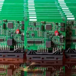
8-Layer PCB Prototype Fabrication: Lamination to Copper
An eight-layer board is not simply a six-layer stack with two more cores. Once the layer count rises, the fabrication route gains a full lamination cycle, the inner cores must be treated before they are bonded, and the plated barrels become long enough that the plating bath has to work harder to reach the centre of the hole. Understanding that sequence is what lets a designer choose a stack that the shop can actually build. This walkthrough follows an 8-layer PCB prototype fabrication order from inner-layer oxidation through lamination, drilling and outer-layer imaging.
What changes when the layer count reaches eight
A double-sided board is a single dielectric with copper on both faces. A multilayer board stacks several routing layers, each pair separated by a dielectric that can be made very thin, and the electrical connection between them is made through plated barrels that cross the board. At eight layers the stack typically contains three or four cores bonded by prepreg, and the sub-assemblies must be finished, tested and oxidised before the final press. The extra steps are not optional; skipping or shortening them is what produces delamination and barrel cracks later.
Brown oxide treatment before lamination
Finished inner layers are always oxidised before they go into the press. Brown oxide treatment, known as black oxide when the coating is predominantly the black cupric form, serves several purposes at once. It removes oils and contamination from the copper surface, increases the effective surface area of the foil so resin can penetrate and interlock with it, and changes a non-polar copper surface into a polar one. Those polar oxide bonds are what give the interface its strength. The oxide also resists moisture during the high-temperature press cycle, which lowers the probability of separation between the copper and the resin. A board that was never oxidised may look fine after pressing and still delaminate after reflow.
Lamination, symmetry and resin flow
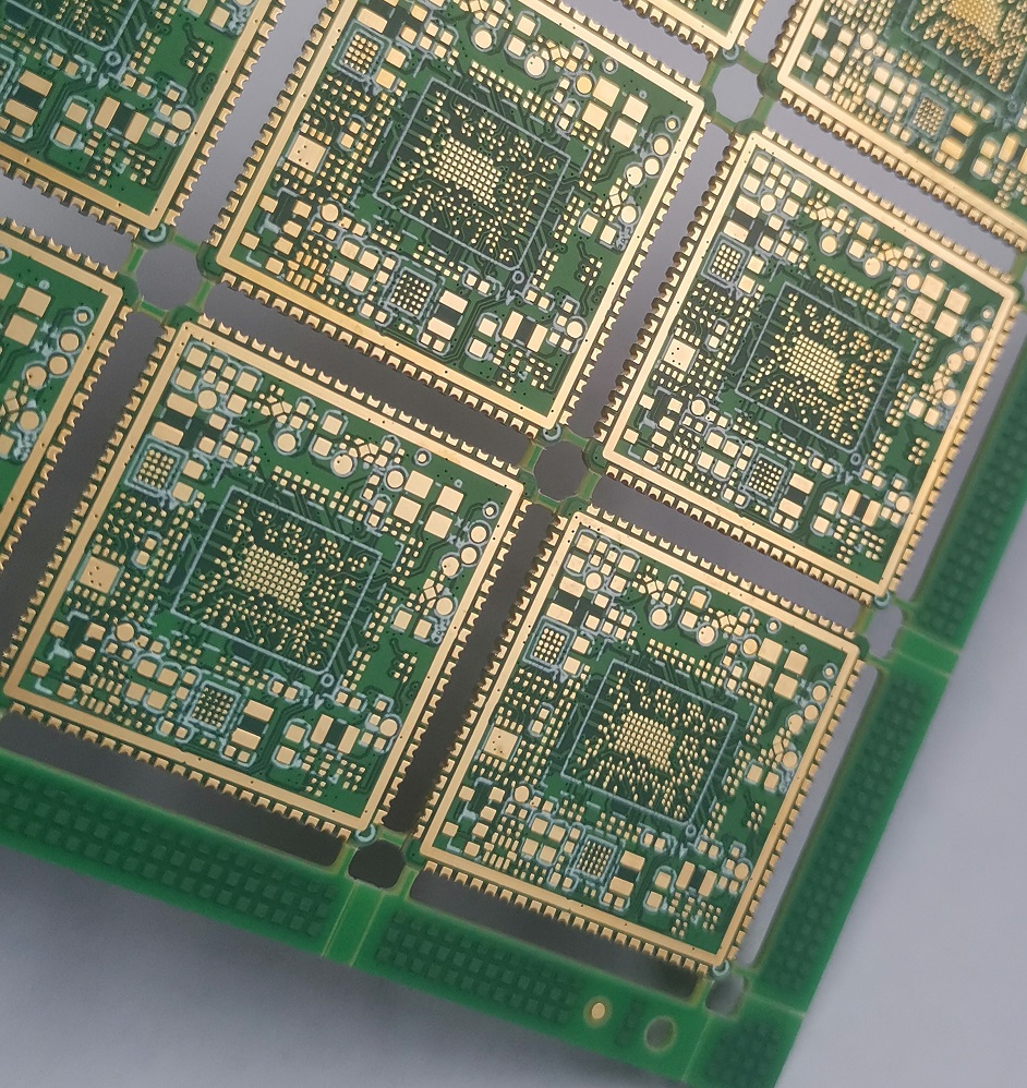
Lamination bonds the stack with B-stage prepreg. Under heat and pressure the resin melts, flows into the copper topography and cures, and the bond forms through diffusion and interlocking of large molecules across the interface. The press is loaded in a defined order: copper foil, prepreg, inner cores, stainless steel separator, kraft paper and outer steel plate, with panels taller than six layers typically pre-stacked before they enter the press.
Two design variables dominate the result. The first is symmetry. The panel sees pressure and temperature, so residual stress remains in the finished board; if the two sides of the stack are not balanced, the stresses differ and the board bows, which compromises assembly and can crack the barrels. The second is copper distribution. Where copper is heavy the resin flows more slowly than in sparse areas, so the finished dielectric is slightly thicker under dense copper and thinner where copper is scarce. Both effects are managed at design time by keeping the stack symmetric and the copper distribution as even as the function allows.
Drilling, de-smear and hole metallization
After pressing, the panel is drilled and the barrels are metallised. The base material is a composite of copper foil, woven glass and epoxy, so a drilled wall exposes all three, and the plating process has to cover that mixed cross-section with a uniform, thermal-shock-resistant copper layer. The sequence runs in three parts: de-smear to remove the resin smear left by drilling, electroless copper to make the wall conductive, and panel plating to build the copper to a workable thickness.
Via aspect ratio and what it limits
The controlling capability figure is the via aspect ratio, the board thickness divided by the drilled hole diameter. As boards get thicker and holes get smaller, chemistry struggles to exchange inside the barrel. Plating equipment uses vibration and pressure to push chemistry toward the centre, but a concentration gradient still leaves the middle of a deep barrel thinner than the ends. That thin section becomes a latent open circuit: it passes electrical test, then fails when the board sees voltage stress or thermal cycling. The value must be checked for through vias and for blind and buried vias, and it must be compared against the fabricator capability before the stack is fixed.

Outer layer dry film and pattern plating
Outer-layer imaging works on the same principle as inner-layer imaging, using a photosensitive dry film and an exposure tool to transfer the pattern. In a subtractive process the outer film behaves as a negative resist: the areas that remain after development cover what will become the traces, the unexposed film is stripped away, and the exposed copper is etched. Because those traces are plated up before etching, the process is often called pattern plating, and the plating current must be uniform across the panel or the trace widths will vary from centre to edge. Reviewing the multilayer prototype requirements before release avoids most of the surprises at this stage.
Keeping the stack buildable
Most first-pass problems on an eight-layer prototype trace back to the stack rather than to the routing. A stack that alternates signal and plane layers, keeps the dielectric thicknesses symmetric about the centre, and respects the aspect ratio limit will laminate, drill and plate predictably. A stack that ignores one of those rules will pass design rule check and still cause trouble in the press or the plating line. Compare the intended stack against the balanced stack-up rules and against layer stack-up practice for one to eight layers, then confirm the aspect ratio with the fabricator. gopcb reviews the stack with the customer before the inner layers are released, because that is the last point where a change costs nothing.
Inner-layer imaging, etching and inspection
The inner cores are built before anything is pressed, and their quality sets the ceiling for the finished board. A photosensitive dry film is laminated to the copper, exposed through the artwork and developed, leaving resist only where copper must survive the etch. After etching and resist stripping, the core carries the final trace pattern for that layer. Because a defect here is buried forever once the stack is bonded, each core is inspected optically and measured against the impedance coupon before it enters the oxidation line. Registration targets are added at the same time so that every layer can be aligned to a common datum during pressing and drilling. When you approve an eight-layer stack, you are approving the tolerance stack-up of four separate imaging steps; that is why inner-layer registration allowance, not routing density, often determines the finest feature the board can carry.
FAQ
Is brown oxide treatment required on every inner layer? Yes. Any inner core that will be bonded into the stack must be oxidised before lamination. Without it the copper-resin interface has lower strength and is far more likely to separate during reflow or thermal cycling.
Why does my eight-layer board bow after pressing? The stack was not symmetric, so the residual stress on one side differs from the other. Balance the dielectric thicknesses and the copper distribution about the centre line, and the bowing disappears without changing the process.
How do I know the aspect ratio is safe? Ask the fabricator for the maximum ratio the plating line can hold reliably, then compare it with the board thickness divided by the smallest drilled diameter. If the design exceeds it, increase the drill size or reduce the board thickness.