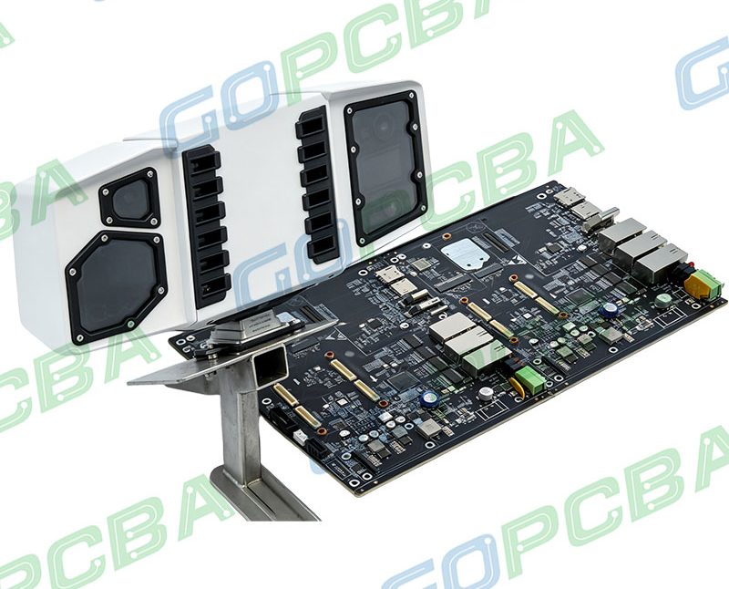
PCB Assembly Capability: What It Means for Your Design
Assembly capability is usually quoted as a list of impressive numbers, and it is more useful to read it as a statement of limits. What matters to a designer is not the maximum placement rate but the smallest package the line can place reliably, the accuracy it holds across a full panel, and the size of the smallest order it will accept without the yield collapsing.
What the Term Covers
PCB assembly capability describes what a factory can build across the range of projects it accepts. It includes the component types it handles, from the smallest chip passives to largest fine pitch area array packages, the assembly processes it runs, including surface mount, through hole and mixed technology, and the accuracy it can hold across the whole panel.
It also includes the flexibility to move from a handful of prototypes to volume production on the same design, and the quality systems that inspect and trace the result. A factory can be strong in one of those dimensions and weak in another, which is why a capability list should always be matched carefully against the actual design rather than accepted as a general claim.
Surface Mount Placement Limits
The smallest passive component a line can place reliably and repeatedly is the number that constrains the whole design. A modern line handles 01005 packages, which are about 0.4 mm by 0.2 mm, but the accuracy needed to place them consistently is much tighter than for 0402 parts, and the placement rate falls as the machine slows to hold that accuracy.
Placement accuracy is usually specified as a tolerance at a stated speed, and the practical question is how that accuracy holds at the edge of the panel, where thermal expansion and mechanical deflection are greatest. Throughput figures are quoted in components per hour, but the rate that matters includes the time spent on fiducial recognition, paste inspection and board transfer. A machine quoted at high speed on a simple panel can be slower than a modest machine on a dense one, so the figure should always be read against the design being built.
Area Array and Fine Pitch Packages
Ball grid array and chip scale packages demand more than accurate placement. They need a stencil that delivers a controlled paste volume to every pad, a reflow profile that brings all the joints to the same thermal state, and an inspection method that can see the joints once they are hidden. X-ray inspection is not optional for these packages.
BGA rework capability matters just as much as placement capability itself. A ball grid array that fails inspection can be reworked only with a dedicated rework station, correct thermal profiling and a replacement ball or a reballed package. A factory that can place these packages but cannot rework them will scrap expensive assemblies, and that cost appears in the quote rather than in the capability list. It is worth asking explicitly what happens to a board that fails X-ray, because the answer reveals whether the process is genuinely controlled or merely performed.
Through Hole and Mixed Technology
Through hole assembly is still required for connectors, power components, transformers and any part that has to resist mechanical load, and it cannot be eliminated by choosing surface mount equivalents in every case. Wave soldering remains the most economical method for a board that is mostly through hole, while selective soldering allows individual joints on a surface mount board to be soldered without subjecting the whole assembly to a wave.
Selective soldering is slower and needs a programme for each board, but it allows a mixed technology assembly to be built with one reflow pass followed by localised soldering at the through hole positions. Where a design has only a few through hole parts, that combination is usually cheaper than wave soldering the entire board, and it avoids subjecting the surface mount joints to a second thermal excursion that they were not designed for.

Paste, Stencil and Profile Control
Paste volume is the variable that most often decides whether a fine pitch joint forms properly. The stencil thickness, aperture size and aperture shape determine the volume deposited, and the print parameters determine how consistently it is deposited across the panel. A factory that monitors paste volume by inspection is far more likely to hold a fine pitch process over a long run, because paste volume drifts as the stencil wears and as the room temperature changes. Inspection closes that loop before the drift becomes a defect.
The reflow profile has to accommodate the thermal mass of the whole assembly, not just the smallest part. Where a board carries both a heavy connector and 01005 passives, the soak has to be long enough to equalise temperature, or the small parts will reach reflow while the heavy joints are still below the activation temperature of the paste.
Inspection and Traceability
The inspection capability has to match the packages used. Optical inspection covers the visible joints, X-ray covers the hidden ones, and in-circuit or flying probe test verifies that the right components are present at the right values, so the three methods answer different questions rather than duplicating each other. A capability list that mentions all three but applies them at different levels of thoroughness and at different sampling rates is not equivalent to one that does.
Traceability is the other half. Being able to identify which paste lot, which component reel and which machine built a specific board is what makes a field failure investigation possible. On regulated products it is a requirement; on consumer products it is a practical tool for finding the cause of a yield drop, as described in placement order and pad positioning.
Matching Capability to a Design
Start from the smallest package and the finest pitch in the design, since those set the placement and inspection requirements. Then check the through hole content and confirm that the factory can handle it, whether by wave, selective soldering or hand work. Then confirm the rework capability for the expensive packages.
Finally, confirm that the factory can scale with the product. A line that is excellent for two hundred pieces may be the wrong choice for twenty thousand, and vice versa. The design rules that keep a board inside those limits are covered in design guidelines for manufacturability.
FAQ
Does a faster placement machine mean better quality? Not necessarily. Placement rate and accuracy trade against each other, and a machine running at maximum speed may hold a wider tolerance. The number to compare is the accuracy specification at the speed the job will run at.
Is hand soldering acceptable on a production board? For a few through hole parts on a small batch, yes, with a defined process and operator qualification. For fine pitch surface mount parts it is not, because the joint quality cannot be controlled or inspected reliably.
What should be asked before placing an order? Ask for the smallest package the line places routinely, the accuracy it holds across a panel, how paste volume is controlled, how area array joints are inspected, and what the rework route is for a failed ball grid array, as summarised in SMT component shift causes.