Electronic Manufacturing Process: 10 Key Steps from DFM to Final Delivery
Electronic manufacturing is the process of producing electronic products used across a wide range of industries, including consumer electronics, industrial automation, automotive electronics, telecommunications, lighting, IoT, computing, robotics, medical equipment, aerospace, and other advanced applications.
A complete Electronic Manufacturing Process involves much more than placing components on a circuit board. It integrates engineering design, PCB fabrication, component sourcing, SMT and through-hole assembly, programming, testing, mechanical integration, quality inspection, packaging, and final delivery.
A well-controlled manufacturing process is essential for achieving consistent quality, reliable performance, manufacturability, and cost efficiency. From the earliest engineering review to final shipment, each stage should be carefully planned and documented.
What Is Electronic Manufacturing?
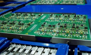
Electronic manufacturing refers to the process of converting an electronic design into a functional physical product through a combination of electronic assembly, mechanical integration, testing, and quality control.
Depending on the product, the manufacturing process may include:
- PCB design and engineering review
- PCB fabrication
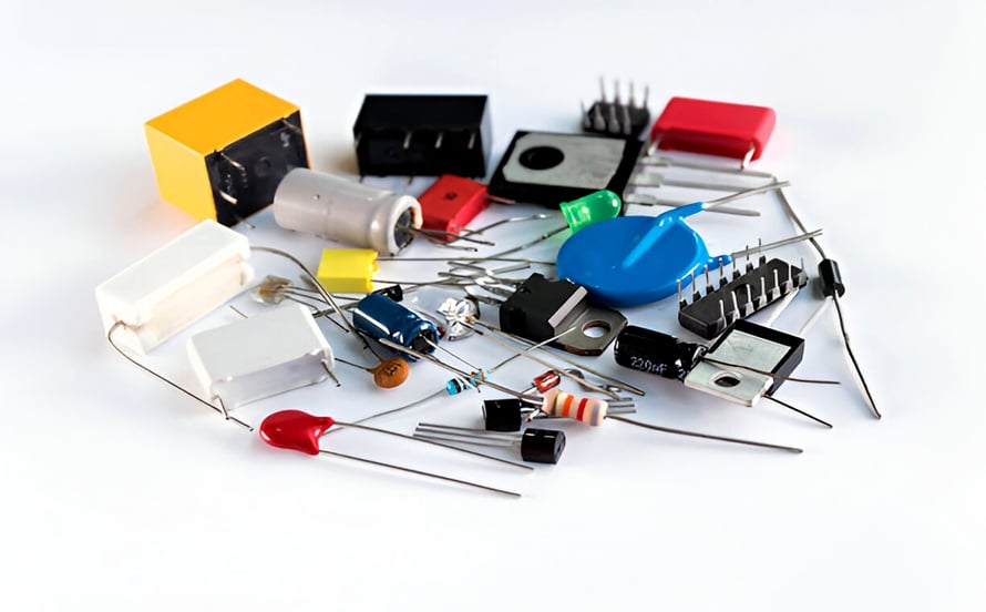
- Component procurement
- SMT assembly
- Through-hole assembly
- Mixed-technology assembly
- IC programming
- PCBA testing
- Box build assembly
- Functional testing
- Burn-in testing
- Final quality inspection
- Custom packaging and shipping
For manufacturers looking for an integrated production partner, PCB Assembly is one of the most important stages because it connects the bare PCB with the electronic components required to create a functional circuit board.
10 Major Steps in the Electronic Manufacturing Process
The exact production flow varies according to PCB structure, component types, product requirements, volume, and testing specifications. However, a typical electronic manufacturing process includes the following 10 stages.
Step 1: DFM Review
Design for Manufacturability (DFM) is one of the most important stages before production begins.
A successful electronic product must not only work according to its electrical specifications; it must also be manufacturable, reliable, testable, and economically viable.
During DFM review, engineers examine the PCB design, component selection, layout, manufacturing data, and assembly requirements to identify potential production problems before they become expensive manufacturing issues.
Typical DFM considerations include:
- PCB pad and footprint design
- Trace width and spacing
- Component placement
- Component clearance
- PCB dimensions and thickness
- Thermal management
- Soldering requirements
- Test-point accessibility
- Mechanical constraints
- EMI and EMC considerations
- Assembly process requirements
DFM is a preventive engineering approach. Identifying design problems before production can reduce rework, scrap, manufacturing delays, and unnecessary design revisions.
Professional PCB Design and engineering support can further improve manufacturability by evaluating the design before PCB fabrication and assembly. PCB Design & Layout services can include layout evaluation, design verification, DFM inspection, and production-data preparation.
Step 2: PCB and Electronic Component Procurement
Once the design has passed engineering review, the next stage is sourcing the PCB and electronic components.
The Bill of Materials (BOM) is the primary document used to identify required components, quantities, manufacturers, part numbers, specifications, and approved alternatives.
Component procurement should consider more than purchase price. Important factors include:
- Component availability
- Lead time
- MOQ requirements
- Manufacturer qualification
- Lifecycle status
- Original versus counterfeit risk
- Alternative component availability
- Cost stability
- Supply continuity
A reliable supply chain can significantly reduce production risks, particularly for products that require long-term manufacturing.
Professional Component Procurement can help manufacturers manage component sourcing, availability, supplier qualification, and production requirements as part of a turnkey manufacturing process.
For critical components, maintaining qualified alternatives can also reduce the risk of production interruptions caused by shortages or unexpected supply-chain problems.
Step 3: PCB Assembly
PCB assembly is the core stage where electronic components are mounted and soldered onto the fabricated PCB.
Depending on the product design, manufacturers may use:
- SMT (Surface Mount Technology)
- THT/DIP (Through-Hole Technology)
- Mixed SMT and THT assembly
- Manual soldering
- Selective soldering
- Wave soldering
- Reflow soldering
A professional PCB Assembly process normally begins with incoming material inspection and production-data verification, followed by solder paste printing, component placement, soldering, inspection, and testing.
The assembly process must be selected according to the PCB structure, component density, package types, and whether components are installed on one or both sides of the PCB.
Reflow Soldering
Reflow soldering is the most common soldering method for SMT components.
During the process, solder paste is deposited onto PCB pads and components are accurately positioned using automated pick-and-place equipment. The assembled PCB then passes through a controlled reflow oven.
A typical reflow profile includes:
- Preheating
- Soaking
- Reflow
- Cooling
The temperature profile must be carefully controlled to achieve reliable solder joints while preventing thermal damage to components and the PCB.
SMT assembly is particularly suitable for high-density electronic designs because it allows manufacturers to place large numbers of compact components with high repeatability.
Wave Soldering
Wave soldering is primarily used for through-hole components.
During wave soldering, the PCB passes over a controlled wave of molten solder. The solder contacts the exposed leads and plated through-holes, creating mechanical and electrical connections.
Wave soldering parameters such as conveyor speed, solder temperature, and wave height must be adjusted according to PCB design, component arrangement, and soldering requirements.
Through-hole components remain important in applications where mechanical strength, connector reliability, or high-current connections are required.
PCB Assembly Processes for Different PCB Designs
Different PCB configurations require different assembly sequences.
Type 1: Single-Sided SMT Assembly
A typical single-sided SMT process is:
Incoming Inspection → Solder Paste Printing → Component Placement → Reflow Soldering → Cleaning → Inspection → Testing → Rework
This process is relatively simple and is suitable for boards where components are mounted on only one side.
Type 2: Double-Sided SMT Assembly
A typical double-sided SMT process is:
Incoming Inspection → B-Side Solder Paste Printing → Component Placement → Reflow → Cleaning → A-Side Solder Paste Printing → Component Placement → Reflow → Cleaning → Inspection → Testing → Rework
Double-sided assembly enables higher component density and more compact electronic products.
Type 3: Single-Sided Mixed Technology Assembly
When SMT and through-hole components are installed on the same side, the process may include:
Incoming Inspection → Solder Paste Printing → SMT Placement → Reflow → Cleaning → DIP/THT Assembly → Wave or Selective Soldering → Cleaning → Inspection → Testing → Rework
Type 4: Double-Sided Mixed Assembly
Double-sided mixed technology boards require more complex process planning.
The sequence may include SMT placement and reflow on one or both sides, followed by DIP/THT insertion and wave or selective soldering.
The optimal process depends on:
- Component size
- Component weight
- PCB orientation
- Component clearance
- Soldering method
- Thermal requirements
- Board thickness
- Production volume
For complex products, Mixed Technology PCB Assembly combines SMT and through-hole technologies to support boards with diverse component requirements.
Step 4: IC Programming
Some electronic products require firmware or software to be programmed into integrated circuits before final testing.
IC programming may involve:
- Microcontroller programming
- Firmware loading
- FPGA programming
- Device configuration
- Calibration data loading
- Serial number programming
A typical programming process includes writing the required software, reading the programmed data, and verifying that the correct firmware has been successfully loaded.
Programming can take place during prototype development as well as volume production.
For production applications, programming should be controlled and traceable so that the correct software version is installed on every product.
Step 5: Functional Testing
Functional testing verifies whether the assembled electronic product operates according to its design specifications.
Unlike visual inspection, functional testing evaluates the electrical behavior and operating performance of the finished assembly.
Typical testing parameters may include:
- Voltage
- Current
- Signal output
- Communication interfaces
- Sensor response
- Switching functions
- Motor operation
- Display functions
- Input/output behavior
A dedicated test fixture can simulate the product’s operating environment and compare actual results against predefined specifications.
Professional PCBA Testing may include electrical testing, fixture-based testing, ICT, FCT, and customized test procedures according to product requirements.
Testing yield can be calculated by comparing the number of passed units with the total number of tested units.
Step 6: Box Build Assembly
After PCB assembly and testing, some products require complete system integration.
Box build assembly combines the PCBA with other electronic, mechanical, and electromechanical components to create a finished product or functional subsystem.
Typical components may include:
- PCBAs
- Power supplies
- Wire harnesses
- Cable assemblies
- Connectors
- Enclosures
- Displays
- Sensors
- Switches
- Fans
- Heat sinks
- Brackets
- Fasteners
The enclosure should provide sufficient mechanical protection and may also need to address thermal management, EMI shielding, environmental protection, and serviceability.
A complete Box Build Assembly process can extend electronics manufacturing from a standalone circuit board to a fully integrated electronic product.
Step 7: Burn-In Testing
Burn-in testing is a reliability screening process designed to identify potential early-life failures.
During burn-in, products may be exposed to controlled electrical loads and elevated temperatures for a specified period.
Typical parameters include:
- Applied voltage
- Operating temperature
- Test duration
- Load conditions
- Environmental conditions
Burn-in equipment should be properly maintained and calibrated to ensure consistent test conditions.
Products that fail burn-in testing can be separated for failure analysis, repair, or further engineering investigation.
Burn-in testing is particularly useful for products where long-term reliability is critical, including industrial electronics, medical equipment, communication systems, and other demanding applications.
Step 8: Custom Packaging
Packaging is an important part of the electronic manufacturing process because the product must remain protected during storage, handling, and transportation.
Packaging should consider the physical characteristics and sensitivity of the product.
Important packaging requirements may include:
- ESD protection
- Mechanical protection
- Moisture protection
- Shock and vibration protection
- Temperature protection
- Dust protection
- Product identification
- Lot and serial-number traceability
For moisture-sensitive electronic products, manufacturers may use moisture barrier bags, desiccants, and humidity indicator cards.
ESD-safe packaging is especially important for sensitive electronic assemblies because uncontrolled electrostatic discharge can damage components even when no visible damage occurs.
Packaging should also comply with applicable customer requirements and transportation regulations.
Step 9: Outgoing Quality Control
Outgoing Quality Control (OQC) is the final quality verification before products leave the manufacturing facility.
The inspection normally verifies:
- Product quantity
- Product identification
- Labels
- Serial numbers
- Physical appearance
- Packaging condition
- Product configuration
- Traceability information
- Test records
- Customer-specific requirements
Skipping final inspection can result in incorrect quantities, product mix-ups, labeling errors, or defective products reaching customers.
A standardized OQC procedure should define inspection methods, sampling levels, acceptance criteria, and documentation requirements.
For complex electronic products, quality control should extend throughout the entire manufacturing process rather than being limited to the final inspection stage.
Step 10: Distribution and Delivery
Distribution is the final stage of the electronic manufacturing process.
After products pass final inspection and packaging, they are prepared for shipment to the customer’s warehouse, production facility, distributor, or final destination.
Effective distribution should protect products against:
- Shock
- Vibration
- Humidity
- Excessive temperature
- Electrostatic discharge
- Mechanical damage
Modern supply-chain systems can also provide shipment tracking, production status updates, inventory management, and delivery information.
A successful distribution process ensures that the correct product reaches the correct destination on time and in acceptable condition.
Key Electronic Manufacturing Design Considerations
A successful manufacturing process begins with a manufacturable PCB design.
Several factors should be considered before production.
1. Component Selection
Component selection should satisfy electrical, mechanical, thermal, reliability, availability, and cost requirements.
PCB footprints must also match the actual component package.
Important considerations include:
- Package dimensions
- Pin pitch
- Lead diameter
- Pad geometry
- Through-hole diameter
- Component height
- Component clearance
- Thermal requirements
Through-hole dimensions should provide sufficient clearance for component leads while maintaining reliable solder penetration and mechanical strength.
2. Component Placement
Component placement has a direct impact on assembly efficiency, inspection, repair, thermal management, and product reliability.
Good layout practices include:
- Avoid unnecessary component crowding.
- Maintain sufficient clearance around large components.
- Keep polarized components consistently oriented where practical.
- Provide sufficient space for connectors and test points.
- Avoid placing small components where they interfere with larger components.
- Consider the accessibility of components during inspection and rework.
For high-density designs, special attention should be given to BGA, QFN, QFP, PLCC, fine-pitch ICs, and small passive components.
3. Selecting the Correct Soldering Process
The appropriate soldering method depends on PCB architecture and component technology.
| PCB Assembly Type | Typical Soldering Process | Typical Application |
|---|---|---|
| Single-sided SMT | Reflow soldering | Simple and compact boards |
| Double-sided SMT | Two-stage reflow | High-density electronics |
| SMT + THT | Reflow + wave/selective soldering | Mixed-technology boards |
| Through-hole assembly | Wave/selective/manual soldering | Mechanically demanding components |
| Complex mixed assembly | Multiple soldering processes | Advanced electronic systems |
Process selection should consider component density, PCB size, thermal mass, component weight, board orientation, and production volume.
4. PCB Material Selection

PCB materials should be selected according to electrical, thermal, mechanical, environmental, and cost requirements.
Common PCB material categories include:
- Standard FR-4
- High-Tg materials
- CEM materials
- Metal-core PCBs
- Ceramic PCBs
- High-frequency materials
- PTFE-based RF materials
- Flexible PCB materials
- Rigid-flex materials
The correct material depends on the application’s operating temperature, frequency, mechanical requirements, signal integrity, and environmental conditions.
For specialized applications, manufacturers should work with the PCB fabricator to confirm the appropriate material and stack-up.
5. PCB Thickness
PCB thickness should be selected according to board dimensions, mechanical strength, component weight, mounting requirements, and application conditions.
Common PCB thicknesses include:
- 0.8 mm
- 1.0 mm
- 1.2 mm
- 1.5 mm
- 1.6 mm
- 2.0 mm
- 2.4 mm
- 3.0 mm
- 3.2 mm and above
Large PCBs or boards supporting heavy components may require greater thickness or additional mechanical support.
The correct thickness should always be determined according to the PCB construction, assembly equipment, mechanical design, and end-use environment.
6. PCB Surface Finish Selection
PCB surface finishing protects exposed copper and helps maintain reliable solderability and electrical performance.
Common PCB surface finishes include:
- HASL
- Lead-free HASL
- ENIG
- OSP
- Immersion Tin
- Immersion Silver
The appropriate finish depends on component density, soldering requirements, environmental conditions, expected product lifetime, electrical performance, and cost.
For fine-pitch components and high-density designs, surface finish selection becomes particularly important because PCB pad quality directly affects soldering reliability.
Why Process Control Matters in Electronic Manufacturing
A reliable electronic manufacturing process is not simply a sequence of machines. It is an integrated system connecting engineering, procurement, manufacturing, inspection, testing, and logistics.
The major benefits of a well-controlled process include:
- Better product consistency
- Lower manufacturing risk
- Improved production yield
- Reduced rework and scrap
- Better component traceability
- More predictable delivery
- Improved product reliability
- Lower total manufacturing cost
Modern PCBA manufacturers increasingly integrate PCB fabrication, component sourcing, SMT/THT assembly, inspection, testing, and final product integration into a single manufacturing workflow.
This one-stop approach can simplify supplier management and improve coordination between engineering and production.
Conclusion
The Electronic Manufacturing Process covers every stage from engineering design to final delivery.
A typical workflow can be summarized as:
DFM Review → PCB & Component Procurement → PCB Assembly → IC Programming → Functional Testing → Box Build Assembly → Burn-In Testing → Custom Packaging → OQC → Distribution
Among these stages, PCB Assembly, component sourcing, engineering review, testing, and quality control are especially important for ensuring that electronic products meet their functional and reliability requirements.
For OEMs and product developers, choosing a manufacturing partner with integrated PCB fabrication, component procurement, SMT/THT assembly, testing, and system integration capabilities can significantly simplify the transition from prototype to production.
A comprehensive manufacturing partner can help manage the complete process—from PCB manufacturing and component sourcing through assembly, inspection, testing, packaging, and final delivery—while maintaining consistent quality and traceability throughout production.