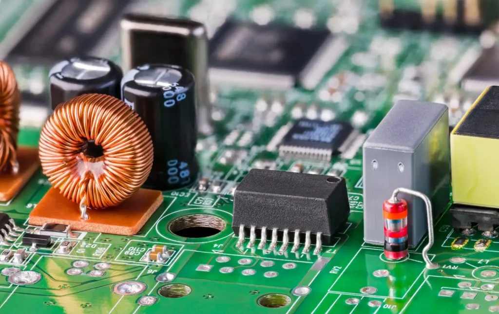
PCB Assembly (PCBA) is a fundamental process in modern electronics manufacturing. It transforms a bare printed circuit board into a functional electronic assembly by mounting and soldering components such as resistors, capacitors, integrated circuits, connectors, sensors, and power devices.
As electronic products become smaller, faster, and more highly integrated, PCB assembly technology has evolved from manual soldering to highly automated production. Modern SMT assembly, THT assembly, automated inspection, electrical testing, component traceability, and engineering services allow manufacturers to achieve higher production efficiency and more consistent quality.
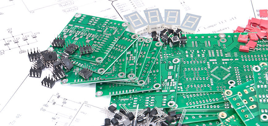
However, reliable PCB assembly involves much more than placing components on a circuit board. PCB design, component sourcing, solder-paste printing, component placement, reflow soldering, inspection, testing, and process control all have a direct impact on the performance and reliability of the finished product.
This guide explains the major types of PCB assembly, PCB assembly process, SMT and THT technologies, quality-control methods, common PCBA defects, manufacturer selection criteria, and Kingda’s PCB assembly capabilities.
What Is PCB Assembly?
PCB Assembly, commonly abbreviated as PCBA, is the process of mounting electronic components onto a bare printed circuit board (PCB) and creating reliable mechanical and electrical connections.
A typical PCB assembly process includes:
PCB Fabrication → Component Sourcing → Solder Paste Printing → Component Placement → Soldering → Inspection → Electrical Testing → Final Assembly
Depending on the application, additional processes may include:
- Programming
- Conformal coating
- Cable and wire-harness assembly
- Mechanical assembly
- Box-build assembly
- Labeling
- Packaging
The exact production workflow depends on the PCB design, component packages, production volume, testing requirements, and application environment.
Types of PCB Assembly
Different electronic products require different assembly technologies. The three most common approaches are SMT PCB Assembly, Through-Hole PCB Assembly, and Mixed Technology PCB Assembly.
SMT PCB Assembly
Surface Mount Technology (SMT) is the dominant PCB assembly method for many modern electronic products.
In SMT assembly, components are mounted directly onto the surface of the PCB without requiring conventional through-holes for each component lead.
Typical SMT components include:
- Resistors
- Capacitors
- Diodes
- QFPs
- QFNs
- BGAs
- CSPs
- LGAs
- Small-outline ICs
- SMD LEDs
Advantages of SMT Assembly
High Component Density
SMT allows many components to be placed in a relatively small area.
High Production Efficiency
Automated pick-and-place machines can install large numbers of components at high speed.
Compact PCB Design
Smaller component packages enable thinner and more compact products.
Consistent Placement Accuracy
Modern vision-guided placement systems provide high positioning accuracy.
Kingda supports SMT assembly for prototype, low-volume, and medium-to-high-volume production, including complex component packages and advanced electronic assemblies. (GoPCBA)
Through-Hole PCB Assembly
Through-Hole Technology (THT) involves inserting component leads through holes drilled in the PCB and soldering them on the opposite side.
THT remains important for components that require strong mechanical support, such as:
- Connectors
- Transformers
- Large capacitors
- Relays
- Power components
- Certain switches
- Mechanically stressed components
Advantages of THT Assembly
THT components can provide strong mechanical connections and may be particularly suitable for products exposed to:
- Vibration
- Mechanical shock
- Thermal cycling
- High insertion forces
THT is commonly found in industrial equipment, power electronics, automotive products, and other applications where mechanical robustness is important.
Mixed Technology PCB Assembly
Mixed Technology PCB Assembly combines SMT and THT components on the same PCB.
This approach is common when a product contains both highly miniaturized surface-mount components and larger mechanically robust components.
The general process may include:
SMT Printing → SMT Placement → Reflow → THT Insertion → Selective/Wave Soldering → Inspection → Testing
Kingda provides SMT, THT, and mixed-technology assembly, with services including wave and selective soldering, AOI, X-ray inspection, first-article inspection, functional testing, and customized packaging. Its published applications include automotive electronics, medical devices, LED lighting, industrial control, communications, and smart-home systems. (GoPCBA)
Advanced PCB Assembly Technologies
As electronics become more compact, manufacturers increasingly use advanced packaging technologies.
Fine-Pitch Assembly
Fine-pitch components require highly accurate:
- Stencil printing
- Component placement
- Pad design
- Reflow profiles
- AOI and X-ray inspection
Kingda states that its assembly capability supports components including 0.35 mm-pitch BGA, 01005 passive components, and fine-pitch components down to 0.38 mm pitch. (GoPCBA)
BGA Assembly
Ball Grid Array (BGA) components provide high I/O density while saving board space.
Because the solder joints are hidden beneath the package, X-ray inspection is commonly used to evaluate solder-joint quality.
QFN and LGA Assembly
Bottom-terminated packages such as QFN and LGA require precise stencil design and reflow control because their solder joints are not fully visible after assembly.
Chip-Scale and Advanced Packaging
More advanced applications may use:
- CSP
- PoP
- Flip-chip
- Chip-scale packaging
- System-in-package technologies
These technologies can reduce package size and increase functionality but require more sophisticated assembly and inspection capabilities.
The PCB Assembly Process
A reliable PCB assembly process requires controlled operations from incoming material inspection through final shipment.
1. Design Review and DFM/DFA
Before production begins, engineers should review the PCB design for manufacturability and assembly.
Important considerations include:
- Component footprints
- Pad dimensions
- Component spacing
- Fiducial marks
- Solder-mask openings
- PCB thickness
- Component orientation
- Thermal considerations
- Test points
- Panelization
DFM (Design for Manufacturability) identifies potential PCB fabrication problems.
DFA (Design for Assembly) evaluates whether components can be assembled efficiently and reliably.
Kingda provides DFM/DFA services, including review of customer design files, BOMs, and manufacturing data before production. (GoPCBA)
2. Incoming Material Inspection
Quality control begins before assembly.
Incoming inspection can verify:
- Bare PCB specifications
- Component part numbers
- Component quantities
- BOM consistency
- Packaging
- Surface condition
- Material certifications
Kingda states that incoming PCBs, electronic components, and production materials are inspected and verified against approved BOMs and manufacturing documentation. (GoPCBA)
3. Solder Paste Printing
For SMT assembly, solder paste is deposited onto PCB pads using a stencil.
Printing quality depends on:
- Stencil aperture design
- Paste condition
- Board flatness
- Printing pressure
- Printing speed
- Alignment accuracy
A poorly controlled printing process can create defects before components are even placed.
Typical solder-paste problems include:
- Insufficient solder
- Excessive solder
- Offset printing
- Bridging
- Uneven deposition
4. Solder Paste Inspection
SPI (Solder Paste Inspection) checks the solder-paste deposition before component placement.
SPI can identify problems such as:
- Paste-volume variation
- Pad offset
- Missing paste
- Excess paste
- Insufficient paste
Early detection helps prevent downstream soldering defects.
Kingda lists 3D SPI among its inspection capabilities. (GoPCBA)
5. Component Placement
Automated pick-and-place machines position components according to the approved production files.
Placement systems use vision recognition to verify:
- Component orientation
- Component position
- Reference marks
- Package geometry
High-density assemblies require particularly precise placement because even small positional errors can affect solder-joint formation.
6. Reflow Soldering
After component placement, the PCB enters a reflow soldering oven.
A typical reflow process includes:
Preheat → Soak → Reflow → Cooling
The thermal profile should be matched to:
- Solder-paste chemistry
- PCB material
- Component specifications
- Board thermal mass
- Assembly configuration
An inappropriate profile can cause:
- Poor wetting
- Tombstoning
- Solder bridging
- Component damage
- Voiding
- Head-in-pillow defects
7. THT Insertion and Soldering
For mixed-technology assemblies, through-hole components are inserted after or around the SMT process.
Depending on the design, manufacturers may use:
- Wave soldering
- Selective soldering
- Manual soldering
- Automated insertion
Selective soldering is particularly useful when THT components must be soldered without unnecessarily exposing nearby SMT components to heat.
8. AOI Inspection
Automated Optical Inspection (AOI) uses cameras and software to inspect assembled PCBs.
AOI can identify:
- Missing components
- Incorrect components
- Component misalignment
- Polarity errors
- Solder bridges
- Tombstoning
- Visible solder defects
AOI can provide fast, repeatable inspection across high-volume production.
9. X-Ray Inspection
X-ray inspection is especially useful for hidden solder joints.
Typical applications include:
- BGA
- QFN
- LGA
- Bottom-terminated packages
- Complex multilayer assemblies
X-ray can identify:
- Voids
- Hidden bridges
- Insufficient solder
- Open joints
- Package alignment problems
Kingda lists X-ray inspection as part of its PCBA quality system. (GoPCBA)
10. Electrical Testing
Electrical testing verifies whether the assembled PCB behaves correctly at the electrical level.
Common methods include:
ICT
In-Circuit Testing (ICT) can verify components and electrical connections using a test fixture.
Flying Probe Testing
Flying probe testing is commonly useful for prototypes and low-volume production because it generally does not require a dedicated fixture.
Functional Testing
Functional Testing (FCT) evaluates whether the completed PCB performs its intended functions.
Depending on the application, testing may include:
- Voltage
- Current
- Communication interfaces
- Sensor operation
- Motor control
- Display operation
- Power management
- Programming
- Wireless functions
Kingda provides ICT, FCT, and customized testing solutions as part of its PCB assembly service. (GoPCBA)
Key PCB Assembly Quality Control Steps
A comprehensive quality-control system should monitor production throughout the entire assembly process.
IQC — Incoming Quality Control
Checks incoming materials before production.
SPI — Solder Paste Inspection
Verifies solder-paste deposition.
SMT/THT Process Control
Monitors:
- Component placement
- Reflow
- Wave soldering
- Selective soldering
- Manual operations
AOI — Automated Optical Inspection
Detects visible assembly defects.
X-Ray
Inspects hidden solder joints.
ICT/FCT
Verifies electrical and functional performance.
OQC — Outgoing Quality Control
Final inspection confirms that products meet approved specifications before shipment.
Kingda’s published quality-control flow is:
IQC → SPI → SMT/THT Assembly → AOI → X-Ray → ICT/FCT → OQC. (GoPCBA)
Common PCB Assembly Defects and Solutions
Even highly automated production can generate defects if process parameters are not properly controlled.
1. Solder Bridges
A solder bridge occurs when solder unintentionally connects two adjacent pads or leads.
Common Causes
- Excess solder paste
- Incorrect stencil apertures
- Excessive component offset
- Incorrect reflow parameters
- Insufficient pad spacing
Solutions
- Optimize stencil design
- Control solder-paste deposition
- Improve placement accuracy
- Optimize the reflow profile
- Perform SPI and AOI
2. Cold Solder Joints
A cold solder joint can occur when solder does not properly wet the pad or component termination.
Potential causes include:
- Incorrect temperature profile
- Poor surface condition
- Insufficient thermal exposure
- Contaminated surfaces
Solutions
- Validate the reflow profile
- Maintain proper solder-paste storage
- Keep PCB surfaces clean
- Monitor solder-joint quality
3. Tombstoning
Tombstoning occurs when one end of a small passive component lifts during reflow.
It can result from:
- Uneven heating
- Unequal solder-paste volume
- Pad-design differences
- Component placement errors
Solutions
- Optimize pad geometry
- Balance solder-paste deposition
- Improve thermal uniformity
- Optimize component placement
- Validate the reflow profile
4. Component Misalignment
Incorrect placement can cause:
- Poor solder connections
- Short circuits
- Open circuits
- Functional failures
High-accuracy placement equipment and AOI help prevent and detect these problems.
5. Solder Voiding
Voids may form inside solder joints during reflow.
For certain power components or thermal connections, excessive voiding can influence thermal and mechanical performance.
Stencil design, solder-paste selection, reflow parameters, and component-pad design should therefore be optimized according to the application.
6. Head-in-Pillow Defects
Head-in-pillow (HiP) defects are particularly associated with BGA assembly.
The solder ball and solder paste may fail to form a reliable joint during reflow.
Potential causes include:
- Warpage
- Oxidation
- Insufficient solder paste
- Reflow-profile problems
- Package-board interaction
X-ray inspection can help identify these hidden defects.
How to Choose the Right PCB Assembly Manufacturer
Selecting the right PCB assembly manufacturer is a strategic decision that can directly influence product quality, cost, lead time, and reliability.
1. Manufacturing Capability
Evaluate whether the supplier supports:
- SMT
- THT
- Mixed technology
- BGA
- QFN
- Fine-pitch components
- Flexible PCBs
- Rigid-flex PCBs
- HDI PCBs
- High-speed PCBs
Kingda offers PCB assembly for rigid, flexible, and rigid-flex boards and supports prototype through high-volume production. (GoPCBA)
2. Engineering and DFM Support
A capable PCB assembly supplier should provide engineering input before production.
Look for support in:
- DFM
- DFA
- BOM review
- PCB layout review
- Component selection
- Panelization
- Test-point optimization
Early engineering involvement can prevent expensive redesigns.
3. Component Sourcing
Component availability can have a major impact on production schedules.
A reliable turnkey PCB assembly supplier should have established sourcing channels and systems for:
- Component availability
- BOM management
- Alternative parts
- Inventory management
- Counterfeit-risk control
Kingda provides global component procurement and supply-chain management and uses an ERP-based inventory system to support PCBA projects. (GoPCBA)
4. Inspection and Testing
Do not evaluate a PCB assembly supplier based only on SMT machine count.
A complete production system should also include:
- SPI
- AOI
- X-ray
- ICT
- FCT
- First Article Inspection
Kingda publicly lists all of these inspection and testing capabilities. (GoPCBA)
5. Quality Certifications
Depending on the target application, relevant certifications may include:
- ISO 9001
- IATF 16949
- ISO 13485
- ISO 14001
- UL
- Applicable IPC standards
Kingda reports IATF 16949:2016, ISO 13485:2016, ISO 9001:2015, ISO 14001:2015, and UL qualifications, and states that it is an IPC member. (GoPCBA)
6. Traceability
Traceability becomes especially important for automotive, medical, industrial, and other high-reliability applications.
A strong traceability system should allow manufacturers to track:
Components → PCB → Production Process → Inspection → Testing → Shipment
Kingda states that its manufacturing and ERP systems support production traceability throughout the product lifecycle. (GoPCBA)
Why Choose Kingda for PCB Assembly?
Kingda is a one-stop PCB and PCBA manufacturing provider founded in 2013. Its published capabilities integrate PCB design and fabrication, component procurement, SMT, DIP/THT, finished-product assembly, and testing. (GoPCBA)
One-Stop PCB and PCBA Manufacturing
Kingda provides an integrated workflow:
PCB Design → PCB Fabrication → Component Procurement → SMT/THT Assembly → Inspection → Testing → Box Build
This reduces the need to coordinate multiple suppliers and allows PCB fabrication and assembly requirements to be managed through one manufacturing partner. (GoPCBA)
Prototype to High-Volume Production
Kingda provides rapid PCBA prototyping, low-volume production, and high-volume production, supporting different stages of the product lifecycle. (GoPCBA)
Advanced SMT and THT Capabilities
Kingda supports advanced SMT packages, BGA assembly, fine-pitch components, THT, wave soldering, and selective soldering.
Its published PCB assembly facility supports 0.35 mm-pitch BGA, 01005 passive components, and fine-pitch components down to 0.38 mm pitch. (GoPCBA)
Comprehensive Quality Control
Kingda integrates inspection and testing throughout production:
IQC → SPI → AOI → X-Ray → ICT/FCT → OQC
This approach helps identify manufacturing problems at different stages instead of relying solely on final inspection. (GoPCBA)
Engineering Support
Kingda provides DFM/DFA, BOM review, manufacturing optimization, component procurement, and technical support, helping customers identify potential manufacturing problems before production. (GoPCBA)
Global Component Procurement
Kingda provides component sourcing and inventory-management services, with an ERP system used to provide inventory information and support procurement management. (GoPCBA)
Industry Experience
Kingda states that its customers and applications include:
- Medical electronics
- Automotive electronics
- Industrial automation
- Artificial intelligence
- Smart home
- Security
- Electric power
- Communications
It also showcases applications including medical ventilator electronics, AI edge-computing boards, network switches, BMS systems, RF filtering PCBA, industrial data acquisition, and intelligent motion-control systems. (GoPCBA)
PCB Assembly for Different Industries
Medical Electronics
Medical PCB assembly requires high reliability, traceability, and controlled manufacturing processes.
Kingda reports ISO 13485 certification and provides PCB assembly for medical products including diagnostic and respiratory equipment. (GoPCBA)
Automotive Electronics
Automotive PCB assembly requires robust process control and quality management.
Kingda reports IATF 16949 certification and provides PCB assembly for automotive electronics. (GoPCBA)
Industrial Automation
Industrial PCBA applications may include:
- PLC systems
- Industrial controllers
- Machine vision
- Data acquisition
- Motion control
- Robotics
AI and Computing
High-performance computing and AI products require advanced PCB technologies, high-density SMT assembly, thermal management, and reliable high-speed interconnections.
Kingda lists AI edge-computing boards, GPU-related applications, machine vision, robotics, and intelligent automation among its manufacturing capabilities and applications. (GoPCBA)
Future Trends in PCB Assembly
AI-Assisted Manufacturing
AI and data analytics are increasingly being used for:
- Defect recognition
- Predictive maintenance
- Production optimization
- Automated inspection
- Process monitoring
Smaller Components
Continued miniaturization is increasing demand for:
- 01005 components
- Fine-pitch BGAs
- QFNs
- CSPs
- HDI PCB structures
Smart Factory Manufacturing
Modern PCB assembly facilities increasingly integrate:
- Automated production equipment
- MES/ERP systems
- Real-time production monitoring
- Automated inspection
- Digital traceability
Higher Reliability Requirements
Automotive, medical, aerospace, AI, and industrial applications continue to require more comprehensive:
- Testing
- Documentation
- Traceability
- Process validation
- Quality management
Conclusion
PCB Assembly is a complex manufacturing process that combines PCB technology, component sourcing, precision SMT/THT assembly, soldering, inspection, testing, and process management.
The foundation of reliable PCBA production can be summarized as:
Good PCB Design + DFM/DFA + Reliable Components + Precision Assembly + Comprehensive Inspection + Electrical Testing + Traceability
SMT remains the primary technology for many modern electronic products, while THT and mixed-technology assembly remain essential for products requiring mechanical strength or specialized components.
Quality-control technologies such as SPI, AOI, X-ray, ICT, and FCT provide different layers of verification, helping manufacturers detect defects before products reach customers.
For companies seeking a reliable PCB assembly manufacturer, Kingda provides an integrated PCB fabrication, component procurement, SMT/THT assembly, testing, and final product integration service. The company supports prototypes, low-volume production, and high-volume manufacturing while providing DFM/DFA engineering support and comprehensive quality control. (GoPCBA)
With quality systems including IATF 16949, ISO 13485, ISO 9001, ISO 14001, and UL qualifications, Kingda is positioned to support demanding automotive, medical, industrial, AI, communication, power, and consumer-electronics projects. (GoPCBA)