Lead-Free PCB Assembly
RoHS-Compliant PCB Assembly for Reliable Electronics Manufacturing
- One-stop PCB manufacturing, component sourcing, and assembly solutions
- SMT, through-hole, and mixed technology assembly
- Lead-Free PCB Assembly compliant with RoHS requirements
- Quality-controlled manufacturing and inspection processes
- Prototype, low-volume, and production-volume assembly
- AOI, X-ray, ICT, functional testing, and other inspection options
Lead-free manufacturing has become an important requirement for electronics products sold in regulated global markets. Our Lead-Free PCB Assembly services are designed to help customers manufacture reliable electronic products while meeting applicable environmental and material requirements.
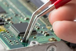
By combining controlled soldering processes, qualified materials, experienced engineering teams, and systematic quality inspection, we support lead-free PCBA production from prototypes through volume manufacturing. Our capabilities cover SMT, through-hole, and mixed technology assemblies for applications including industrial electronics, medical equipment, automotive electronics, communications, consumer electronics, and other demanding products.
What Is Lead-Free PCB Assembly?
Lead-Free PCB Assembly refers to the assembly of electronic components onto a printed circuit board using solder materials that do not intentionally use lead as the primary alloying element.
Traditional tin-lead solder has been widely used because of its excellent wetting characteristics, relatively low melting temperature, and proven reliability. However, environmental regulations have significantly increased the adoption of lead-free soldering throughout the electronics manufacturing industry.
Today, lead-free solder alloys such as SAC305 are widely used for SMT and other electronic assembly applications. SAC305 typically contains approximately 96.5% tin, 3% silver, and 0.5% copper.
The exact solder alloy and process parameters should be selected according to the PCB material, component specifications, thermal requirements, product design, and applicable manufacturing standards.
For customers requiring a complete manufacturing solution, our PCB Assembly Services can integrate PCB assembly with component sourcing, inspection, testing, and other production services.
Common Lead-Free Solder Materials
Different assembly processes may require different solder materials. Common examples include:
SMT Solder Paste
Lead-free solder paste is commonly used for surface mount assembly. SAC-family alloys are widely adopted because they provide a practical balance of solderability, mechanical reliability, thermal performance, and manufacturing cost.
Wave Soldering Solder
Lead-free solder bars used for wave soldering commonly use tin-based alloys with copper and other alloying elements. The specific alloy should be selected according to the equipment, PCB design, component requirements, and soldering process.
Lead-Free Solder Wire
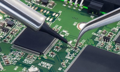
Lead-free solder wire is used for manual soldering, rework, repair, and certain through-hole assembly operations. Flux compatibility and soldering temperature must be properly controlled to achieve reliable joints.
Because lead-free soldering generally requires higher process temperatures than traditional tin-lead soldering, thermal management is an important consideration during PCB assembly.
When Should You Use Lead-Free PCB Assembly?
Lead-Free PCB Assembly is particularly suitable when the finished electronic product must comply with applicable environmental regulations or customer-specific material restrictions.
Lead-free manufacturing is commonly selected when:
- The product is intended for markets with RoHS-related requirements.
- Customers require restricted-substance compliance.
- The product is designed for international distribution.RoHS PCB Assembly
- The end customer specifies lead-free materials and processes.
- Environmental responsibility is an important part of the product strategy.
- The product uses a supply chain that requires lead-free components and materials.
- Long-term manufacturing consistency and material traceability are important.
Lead-free assembly has become a mainstream manufacturing approach rather than a niche production option. However, the correct solder alloy, PCB material, components, and thermal profile must be evaluated for every project.
Lead-Free PCB Assembly vs. Leaded PCB Assembly
The main difference between lead-free and leaded assembly is the solder alloy and the associated manufacturing process.
1. Environmental and Regulatory Requirements
Lead-free soldering helps manufacturers meet restricted-substance requirements in markets where applicable regulations limit the use of lead and other hazardous substances.
RoHS compliance should not be assumed simply because a solder alloy is described as “lead-free.” Compliance depends on the materials used throughout the product and the applicable regulatory limits.
2. Solder Alloy Composition
Traditional leaded solder commonly uses tin-lead alloys such as Sn63/Pb37.
Lead-free assembly typically uses tin-based alloys such as SAC305 or other lead-free formulations. The exact composition varies according to the application and soldering process.
3. Melting and Process Temperature
Traditional Sn63/Pb37 solder melts at approximately 183°C.
Many SAC lead-free alloys have higher melting temperatures, generally around 217–221°C. As a result, lead-free reflow and soldering processes normally require higher temperature profiles.
The actual process temperature should always be determined from the solder manufacturer’s specifications, component temperature ratings, PCB material characteristics, and the validated assembly profile.
4. Manufacturing Cost
Lead-free solder alloys may have higher material costs because some formulations contain relatively expensive alloying elements such as silver.
However, total PCB assembly cost depends on much more than solder price. Component costs, PCB fabrication, tooling, labor, testing, yield, production volume, and supply-chain conditions can have a much greater effect on the final manufacturing cost.
How Can You Identify Lead-Free PCB Assembly?
It is difficult to reliably determine whether a PCB assembly is lead-free simply by looking at the finished board.
Visual Appearance
Lead-free solder joints may appear somewhat duller or more matte than traditional leaded solder joints. However, appearance is not a reliable method for determining material composition.
Different solder alloys, fluxes, PCB finishes, component finishes, and process conditions can produce different visual results.
Material Composition
The most reliable approach is to verify the material documentation and manufacturing records.
For regulated products, manufacturers may use supplier declarations, material declarations, certificates, or laboratory analysis to verify restricted-substance compliance.
Manufacturing Documentation
BOM records, solder material specifications, component documentation, PCB material information, and production records can provide stronger evidence of compliance than visual inspection alone.
For customers requiring a controlled sourcing process, Components Procurement can help integrate component sourcing into the overall PCBA manufacturing workflow.
Six Important Factors in Lead-Free PCB Assembly
Producing reliable lead-free assemblies requires careful control of the entire manufacturing process.
1. Control the Wave Soldering Process
Through-hole components may require wave or selective soldering. Solder temperature, contact time, conveyor speed, flux application, and PCB preheating must be controlled according to the process specification.
2. Control Solder and Flux Quantity
Too much solder or flux can cause defects, while insufficient solder or flux may result in poor wetting, insufficient hole fill, solder bridges, or unreliable connections.
3. Control Manual Soldering Temperature
Manual soldering and rework require appropriate soldering iron temperature and contact time. Excessive heat can damage components, PCB pads, or laminate materials.
4. Verify Lead-Free Materials
The PCB, components, solder, flux, and other relevant materials should be verified against the customer’s material and compliance requirements.
5. Maintain Process Consistency
Stable personnel, standardized work instructions, controlled equipment parameters, and documented process procedures help reduce manufacturing variation.
6. Use Appropriate Inspection and Testing
Lead-free assembly should be supported by inspection and testing appropriate to the product. Depending on the design, this may include SPI, AOI, X-ray inspection, ICT, functional testing, and final visual inspection.
Our SMT Assembly capabilities support precision surface-mount manufacturing for complex PCB designs, including prototype and production requirements.
Why Does Leaded PCB Assembly Still Exist?
Although lead-free manufacturing has become widespread, leaded soldering can still be encountered in certain applications.
Special Product Requirements
Some legacy products, specialized applications, or customer-defined manufacturing requirements may still specify leaded solder.
Certain components or assemblies may also have thermal limitations that need to be considered when selecting a soldering process.
Cost Considerations
Some lead-free alloys can be more expensive than traditional tin-lead solder. However, material price alone should not determine the soldering process because regulatory requirements, product reliability, lifecycle requirements, and customer specifications must also be considered.
Regional Requirements
Not every market has identical environmental regulations. Product manufacturers must determine the requirements applicable to their target markets and customers.
For most new commercial electronics products intended for international markets, lead-free manufacturing is increasingly the preferred approach.
Choosing a Lead-Free PCB Assembly Manufacturer
Selecting the right manufacturing partner is important because lead-free assembly requires more than simply replacing leaded solder with a lead-free alloy.
A capable manufacturer should be able to manage:
- PCB fabrication and material selection
- Component sourcing
- BOM verification
- DFM review
- SMT assembly
- Through-hole assembly
- Reflow soldering
- Wave or selective soldering
- AOI inspection
- X-ray inspection
- Electrical testing
- Functional testing
- Traceability and production documentation
For projects requiring both surface-mount and through-hole components, Through-Hole PCB Assembly can be combined with SMT processes to create a complete mixed-technology manufacturing solution.
Lead-Free PCB Assembly Process
A controlled manufacturing process helps ensure consistent quality from incoming materials through final shipment.
1. Engineering and DFM Review
Before production, manufacturing engineers review Gerber files, BOMs, pick-and-place data, assembly drawings, and other relevant documentation.
Potential issues involving component spacing, pad design, thermal requirements, solderability, and manufacturability can be identified before production begins.
2. Material Inspection
Incoming PCBs and electronic components are checked against approved production documentation.
Material verification helps prevent incorrect components, damaged materials, or nonconforming parts from entering production.
3. Solder Paste Printing
For SMT assembly, solder paste is applied to PCB pads using a precision stencil printing process.
The printing parameters must be controlled to achieve consistent paste volume and accurate deposition.
4. Component Placement
Automated pick-and-place equipment positions surface-mount components onto the PCB according to the programmed assembly data.
Placement accuracy is particularly important for fine-pitch components, BGA packages, QFN devices, and miniature passive components.
5. Reflow Soldering
The assembled PCB passes through a controlled reflow profile that melts the solder paste and forms reliable solder joints.
Lead-free alloys generally require higher peak temperatures than traditional tin-lead solder, making thermal profiling especially important.
6. Through-Hole Assembly
Through-hole components can be assembled using automated, selective, wave, or manual soldering processes depending on product requirements.
7. Inspection and Testing
After assembly, inspection and testing verify solder quality, component placement, electrical performance, and overall product conformity.
Testing options can include AOI, X-ray inspection, ICT, functional testing, and customer-specific testing procedures.
For projects requiring a complete manufacturing chain, Turnkey PCB Assembly combines PCB fabrication, component procurement, assembly, testing, and related production services through one manufacturing partner.
Key Considerations When Selecting Lead-Free Materials
Lead replacement alloys must meet several important requirements.
Global Availability
The alloy should be commercially available and supported by a stable supply chain.
Recyclability
A practical solder alloy should support responsible material handling and recycling without creating unnecessary complexity.
Low Toxicity
The purpose of lead-free manufacturing is to reduce the use of hazardous substances. Alternative materials should therefore be selected according to applicable environmental and regulatory requirements.
Electronics Compatibility
The solder alloy must provide suitable solderability, mechanical performance, thermal performance, and reliability for SMT, through-hole, repair, and rework applications.
Process Compatibility
The alloy must also work correctly with the PCB surface finish, component finishes, solder paste, flux, reflow equipment, and other materials used in the production process.
Important Considerations in Lead-Free Solder Development
The development and selection of lead-free solder alloys involves balancing several competing requirements.
Solderability
The solder should wet PCB pads and component terminals effectively while minimizing common soldering defects.
Reliability
The solder joint must maintain mechanical and electrical performance throughout the expected operating environment and product lifecycle.
Cost Efficiency
A suitable alloy should provide the required performance without creating unnecessary manufacturing costs.
Equipment Requirements
Lead-free assembly may require higher process temperatures and careful thermal profiling. Reflow ovens, wave soldering equipment, fixtures, and other manufacturing systems must be properly configured.
Compatibility
The solder alloy must be compatible with flux, PCB surface finishes, component finishes, and the overall assembly process.
Lead-Free PCB Assembly Workshop Requirements
A controlled production environment is essential for reliable PCB assembly.
ESD Protection
The production area should use appropriate electrostatic discharge protection measures, including grounded workstations, ESD flooring or mats where required, wrist straps, and controlled handling procedures.
Temperature and Humidity Control
Temperature and humidity should be maintained within the limits appropriate for the materials, equipment, solder paste storage requirements, and manufacturing process.
Clean Production Environment
Production areas should remain clean and organized. Dust, contamination, moisture, and unnecessary materials should be controlled to reduce manufacturing risks.
Safe Production Layout
Production equipment, electrical systems, material storage areas, aisles, emergency exits, and fire protection equipment should be arranged according to applicable safety requirements.
Material Management
PCBs, components, solder materials, semi-finished products, tools, and production equipment should be stored in designated locations with clear identification.
Employee Training
Production personnel should receive appropriate training covering ESD control, equipment operation, soldering procedures, quality requirements, environmental controls, and workplace safety.
Quality Control for Lead-Free PCBA
Quality should be controlled throughout the entire manufacturing process rather than relying only on final inspection.
A typical quality control flow may include:
Incoming Material Inspection → Solder Paste Inspection → SMT/THT Assembly → AOI → X-Ray → ICT/FCT → Final Inspection
Inspection and testing requirements should be customized according to the PCB design, component package types, product application, customer specifications, and applicable industry standards.
For projects requiring additional inspection and electrical verification, PCBA Testing can be incorporated into the manufacturing process to help identify assembly and functional issues before shipment.
Benefits of Lead-Free PCB Assembly
Regulatory Compliance
Lead-free manufacturing can help products meet applicable restricted-substance requirements for regulated markets.
Environmental Responsibility
Reducing the use of lead supports more environmentally responsible electronics manufacturing.
Global Market Compatibility
Lead-free PCBA is widely adopted throughout global electronics supply chains, making it a practical choice for products intended for international distribution.
Modern Manufacturing Compatibility
Modern SMT and PCB assembly equipment is designed to support lead-free production, including controlled reflow, automated inspection, and advanced testing processes.
Consistent Production
With proper engineering and process control, lead-free assembly can provide reliable and repeatable manufacturing performance from prototypes to production volumes.
Frequently Asked Questions
What is lead-free PCB assembly?
Lead-free PCB assembly is the process of mounting electronic components onto a PCB using solder materials that meet applicable lead-restriction requirements rather than traditional tin-lead solder.
Why is lead-free PCB assembly important?
It helps manufacturers address environmental and restricted-substance requirements and supports the production of electronics intended for markets where lead restrictions apply.
How is lead-free PCB assembly manufactured?
The process generally includes engineering review, material inspection, solder paste printing, component placement, reflow soldering, through-hole assembly where required, inspection, electrical testing, and final quality control.
Is lead-free PCB assembly the same as RoHS PCB assembly?
They are closely related but not exactly identical terms. Lead-free soldering addresses the solder material, while RoHS compliance concerns restrictions on specified hazardous substances throughout the applicable product and materials.
What is lead-free PCBA?
Lead-free PCBA is an assembled printed circuit board manufactured using lead-free soldering materials and processes according to the applicable product and compliance requirements.
What are the advantages of lead-free PCBA?
The main advantages include support for applicable environmental requirements, reduced reliance on lead-containing materials, compatibility with modern electronics manufacturing, and suitability for international product supply chains.
Are there disadvantages to lead-free PCB assembly?
Lead-free soldering can require higher process temperatures and more careful thermal management. Some lead-free alloys may also have higher material costs. Proper process engineering is therefore important.
What are the most important factors in lead-free assembly?
Material verification, solder alloy selection, thermal profiling, solder paste control, component compatibility, process stability, inspection, testing, and traceability are among the most important factors.
Can lead-free PCB assembly include SMT and through-hole components?
Yes. Lead-free assembly can include SMT, through-hole, and mixed technology processes, depending on the PCB design and component requirements.
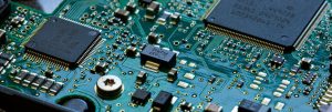
Start Your Lead-Free PCB Assembly Project
Lead-free manufacturing is now an important part of modern electronics production. However, achieving reliable results requires more than simply selecting a lead-free solder alloy. PCB design, materials, component sourcing, soldering profiles, equipment settings, inspection methods, and production controls all contribute to final product quality.
A professional manufacturing partner can help manage these factors from engineering review through assembly, testing, and delivery.
Whether you need prototype production, low-volume manufacturing, or scalable production, our team can support your project with integrated PCB manufacturing, component sourcing, assembly, inspection, and testing.
Submit your Gerber files, BOM, pick-and-place data, and assembly requirements to receive a project evaluation and quotation for your Lead-Free PCB Assembly requirements.