Placement accuracy verification after head calibration

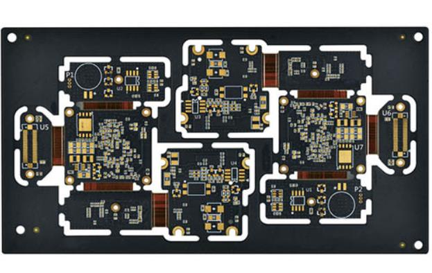
Any-Layer HDI PCB Manufacturing Cost Guide 2026

Any-Layer HDI PCB Manufacturing Cost Guide 2026: From Prototype to Volume Production An any-layer HDI PCB manufacturing cost must be evaluated differently from a standard multilayer board because the design uses laser microvias, sequential build-up, fine lines, and higher-density interconnects. Smartphones, wearables, 5G equipment, automotive electronics, medical devices, and high-performance…
PCB Substrate Materials

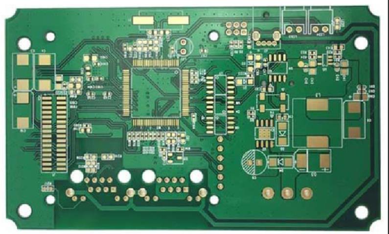
PCB Substrate Materials: Key Material Properties for High-Speed PCB Design

The electrical, mechanical, and thermal behavior of a printed circuit board depends heavily on the materials used in its construction. In addition to copper conductors and electronic components, the selection of PCB Substrate Materials has a direct impact on signal integrity, thermal management, mechanical reliability, and long-term performance. For conventional…
Cadence PCB Design

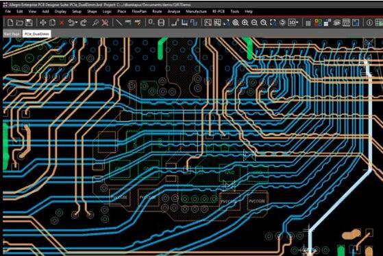
Cadence PCB Design: High-Speed PCB Layout, Routing and Signal Integrity Guide

Cadence is a widely used electronic design automation (EDA) platform that supports many stages of electronic product development, including ASIC design, FPGA development, and printed circuit board design. For complex and high-speed electronic products, Cadence PCB Design provides an integrated environment for schematic capture, component and footprint development, PCB layout,…