Component Spacing Rules For SMT Layout
A component spacing rule defines how close two parts may be placed to each other and to other features on the board. It is written for the process rather than for the circuit, and it exists because assembly equipment, rework tools, heat and inspection all need space that the schematic does not mention.
Spacing rules are often treated as a preference to be relaxed at the end of a layout when space runs out. In practice they are a process requirement, and relaxing them moves the cost from the layout onto the factory floor, where it is far harder to absorb.
Why Spacing Is A Rule And Not A Preference
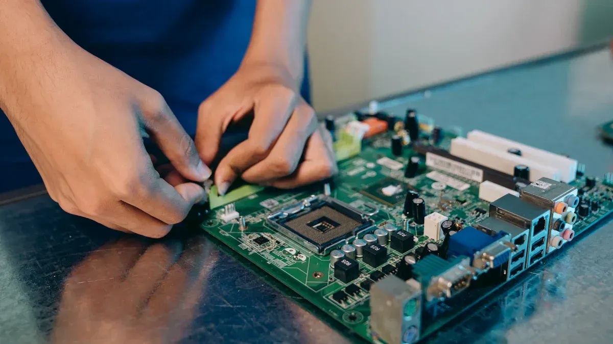
The placement machine needs room for its nozzle and for the vision system, the reflow oven needs a thermal path, the inspection system needs a viewing angle, and a hand rework station needs a soldering iron tip that can reach the joint. Each of those has a physical size, and the spacing rule is derived from it.
A layout that ignores the rules can still be built, but it is built more slowly and with more defects. The extra cost appears as yield loss, as added inspection time and as rework, none of which is visible in a quotation until the boards are in production.
The Courtyard And Its Meaning
The courtyard is the outline drawn around a footprint that includes the component body plus the tolerance for placement and for the manufacturing variation of the part. It is the area that must not overlap the courtyard of another component.
Courtyard rules are defined in the industry standard for footprints, and a common requirement is that courtyards may touch but must not overlap. Where two courtyards overlap, the layout tool should flag it, and that flag should be treated as a real error rather than as a warning.
Spacing For Assembly Equipment
The placement nozzle approaches from above, so the constraint is usually vertical clearance rather than lateral space. A tall component placed next to a short one can block the nozzle path if the difference in height is large and the two are close together.
The vision system adds a lateral constraint of its own. A fiducial or a local alignment mark needs a clear area, and a tall part close to a mark can shadow it and cause a placement error that appears only at high index speed.
Spacing For Rework And Repair
Rework is where spacing rules earn their place. A hot air nozzle has a defined diameter, and a component surrounded by others at close spacing cannot be removed without heating its neighbours as well, which risks disturbing their joints.
The practical figure is a gap of at least 1 mm between the bodies of small chip components, and more around a large device such as a ball grid array or a shielded module. That gap is what allows a nozzle or a shield to be placed without touching anything else.
Thermal Coupling Between Components
Two components placed close together share their heat. A temperature sensitive part next to a power device sees a higher local ambient than the design assumed, and its performance or its life can fall as a result.
The coupling depends on the copper between them as much as on the distance. A wide copper connection carries heat efficiently, while a narrow one and a slot reduce it. Where thermal coupling is a concern, the copper is often the better lever than the spacing. The way copper moves heat is described under copper flooding mesh or solid.
Spacing For Test And Inspection
Automated optical inspection needs a viewing angle, which means it needs space at the side of a component. A tall part with another part pressed against it has a shadowed side that cannot be inspected, and that shadow becomes a blind spot in the program.
Test points need their own clearance, and a probe needs a vertical path down to the pad. A test point under an overhanging component is useless, and the error is usually only discovered when the test fixture has already been built.
Spacing Around Connectors
Connectors need space for the mating part, not only for the connector itself. A cable, a mating header or a card guide occupies volume outside the board outline, and that volume has to be reserved in the layout as a keepout.
The keepout should be taken from the connector drawing and should include the latch or the retention feature. A connector whose latch is blocked cannot be mated reliably, and the fault then appears at the customer rather than in the factory.
Spacing And The Board Edge
Components are normally kept clear of the board edge by at least 0.5 mm, and more where the panel is routed or where a card guide grips the edge. Routing produces a burr at the edge, and a component close to that burr can be damaged when the panel is depanelised.
The edge clearance also matters for the conveyor in the assembly machine, which grips the board by its edges. A component that extends into the grip zone risks damage and can contaminate the conveyor with solder paste. The outline rules behind this are described under board outline and mounting design.
Documenting The Rules
The spacing rules should be written into the design rule set of the CAD tool so that they are checked automatically. A rule that lives only in a document is applied inconsistently, while a rule inside the tool is applied to every placement without fail.
The rule set should distinguish between hard rules, which must never be broken, and soft rules, which can be relaxed for a stated reason. That distinction allows a design to be tight where it has to be without losing control of everything else. How the rules are agreed with the assembler is described under PCBA development process.
Spacing Between Different Package Types
The gap needed between two components depends on their packages as much as on their physical size. A quad flat pack with leads on four sides needs clearance for the lead tips, while a ball grid array needs clearance for the rework nozzle that will be used if the part ever has to be replaced.
A mixed board therefore carries a range of rules rather than one rule. The sensible approach is to set the spacing from the most difficult package in the neighbourhood, and to allow tighter gaps only between parts that are unlikely to need rework during the life of the product.
A shielded module needs more space than its outline suggests, because the shield is a metal can that has to be removed and replaced during rework. The keepout should follow the shield outline rather than the module body, and it should include the height of the can as well as its footprint.
FAQ
What is a typical spacing between chip components? A gap of at least 1 mm between component bodies is a good baseline, and 0.5 mm is sometimes used on a dense board where rework is not expected.
Can courtyards overlap? According to most footprint standards they should not. Touching is normally acceptable, and overlapping indicates that one of the parts will be difficult to place or to rework.
Does spacing affect the board size? It does, because more space per component means a larger board. The trade is between board area and production cost, and production cost is often the larger of the two.