
Copper Balance And Thieving On PCB Layers
Copper balance is the degree to which the copper on a layer is distributed evenly across the panel. It affects two things that matter after the board is finished: the uniformity of the plating that is deposited in the holes, and the flatness of the board after lamination and after reflow.
This article explains why the distribution matters, how thieving and dummy patterns are used to even it out, and how the result is checked before the artwork is released.
Why Copper Distribution Matters
Copper and laminate expand at different rates and they conduct heat differently. A layer with a large copper area on one side of the panel and a sparse area on the other will laminate with different resin flow in the two regions, and after cure the panel holds a built in stress. When the board is later heated, in assembly or in service, that stress is released as movement, and the board bows or twists.
The effect is strongest where the copper is very uneven, such as a board with a large ground plane on one layer and only a few traces on the layer above it. In that arrangement the two layers pull the core in opposite ways and the panel curls. The imbalance also shows up in the finished thickness: resin flows away from a dense copper area and accumulates in a sparse one, so the dielectric thickness varies across the board and the impedance with it. The related question of layer arrangement is treated under balanced stackup and odd layer count.
Plating Current Density
In the plating bath the board is one electrode and the current has to reach every point on the copper surface, including the inside of every hole. The resistance of the path from the bus bar to a hole depends on how much copper is connected to that hole, and therefore on the local copper density. A hole in a dense area is fed by a low resistance path and plates with a higher current density; a hole in a sparse area is fed by a thin trace and plates more slowly.
The result is poor plating uniformity across the panel and between boards, and it is the reason that the thickness is specified at the thinnest point anticipated rather than as an average. Thieving addresses the cause by adding copper in the sparse areas so that the current distribution becomes more even, and the additives in the bath that control the deposit structure are described under electroplating additives for PCB.
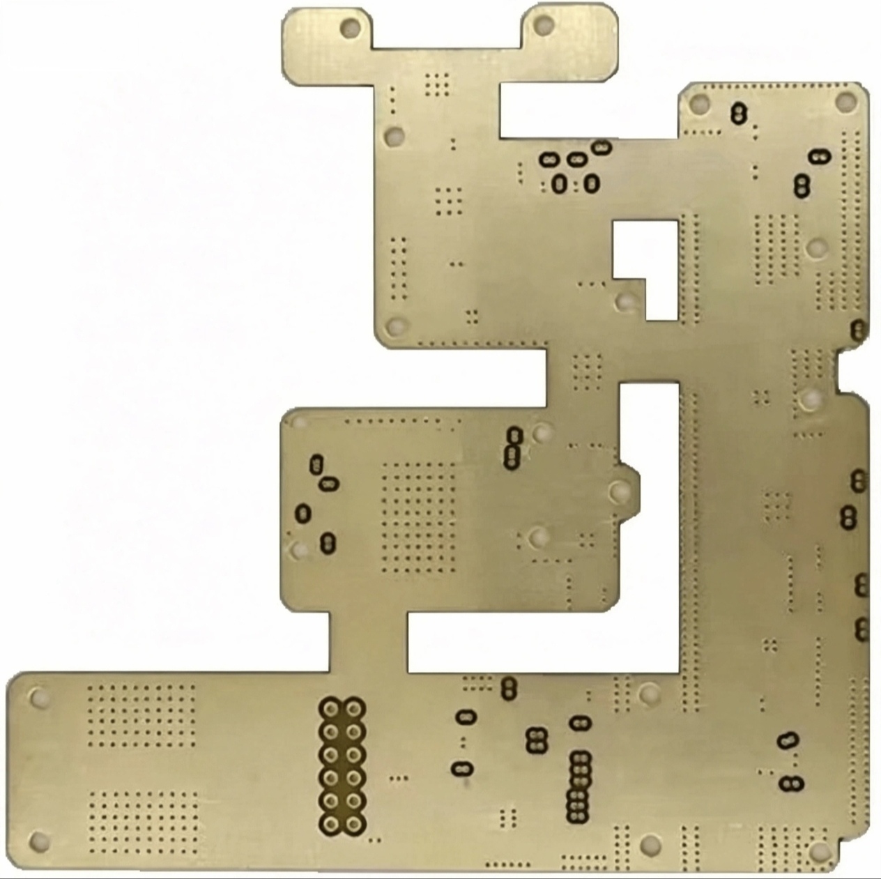
Thieving And Dummy Patterns
Thieving is a pattern of small copper features added to a layer in areas that carry no circuit. The features are isolated from the circuit, connected to no net, and they serve only to change the local copper density. A common form is a grid of small squares or a hatch pattern, sized so that it does not couple to nearby traces and so that it does not become an antenna.
The pattern has to be designed with the same care as the circuit. Features placed close to a sensitive trace add capacitance and change the impedance of that trace; a large solid thieving area next to a signal trace becomes a coupled conductor. This is why thieving is normally a hatched pattern with a defined clearance from the circuit rather than a flood, and why the choice between a mesh and a solid fill for a ground area is worth understanding in its own right, as described under copper flooding: mesh or solid.
Warpage And Layer Symmetry
Warpage is the visible consequence of imbalance, and it is controlled by making the stack symmetrical in two senses. The first is the arrangement of the layers: a stack with two build up layers on one side of the core and three on the other is asymmetric and will curl. The second is the copper content of the layers: a stack that is geometrically symmetric but has a heavy plane on one side and nothing on the mirror layer will also curl, because the two halves of the board have different stiffness and different expansion.
Where a symmetric arrangement is impossible, thieving on the sparse layer is the corrective measure, and it is applied to bring the two halves of the stack closer in copper content. The requirement is expressed as a percentage, and the check is a comparison of the copper area on each layer within a defined region, usually the panel rather than the individual board. The way the laminate behaves when it is heated, and the expansion that drives the movement, are described under PCB dimensional stability and expansion.

Checking Balance Before Release
The check is performed on the finished artwork, layer by layer, in a defined grid across the panel. Each cell of the grid is assigned a copper percentage, and the spread across the panel is compared with a target. A layer that is much denser in one corner than another is flagged, and thieving is added to the sparse corner until the spread comes inside the target.
Two refinements make the check meaningful. The first is to measure over a cell size that is comparable with the plating scale rather than with the whole board, because a panel that is balanced overall can still have a local imbalance that affects the current density at one hole. The second is to check the layers as a stack rather than individually, because two layers that are each mildly imbalanced in opposite directions can cancel while two that are imbalanced in the same direction accumulate.
Limits And Drawbacks
Thieving adds copper, and copper that is added for plating balance is copper that has to be removed by etching, which extends the etch time and consumes etchant. The pattern also changes the appearance of the board and consumes some of the space that could have carried routing, which is why it is normally added to the layers that have the most free area rather than to the dense ones.
There is also a cost in electrical performance where the pattern is applied carelessly. A thieving grid under a high frequency trace changes the effective dielectric environment, and a grid that is connected to ground in one place and floating in another creates a path that was never intended. Where the board carries sensitive analogue or high speed signals, the thieving pattern is designed to avoid those areas entirely, and the balance for those regions is managed by the routing itself rather than by added copper.
FAQ
Does thieving affect the circuit electrically? It can, if it is placed close to a trace or left floating in a location where it couples to a signal. A hatched pattern with a defined clearance and a deliberate connection, or a deliberate isolation, is the safe arrangement.
Is a copper pour the same as thieving? No. A pour is connected to a net for electrical reasons, usually ground, while thieving is added for process balance and is normally isolated from every net.
How much imbalance is acceptable? The target comes from the fabricator, because the acceptable spread depends on its lamination and plating process. A common starting target is to keep the copper content of the densest and the sparsest region of a layer within a few tens of percent of each other.