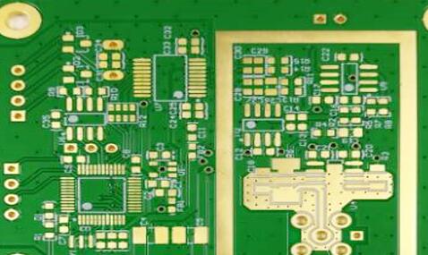
Copper plating is one of the most important processes in PCB Manufacturing. It provides the conductive copper required for circuit formation, through-hole interconnection, and reliable electrical connections between PCB layers. A properly controlled copper plating process also contributes to mechanical strength, solderability, and long-term PCB Reliability.
In modern PCB production, copper deposition is generally divided into two complementary processes: Electroless Copper Plating and Copper Electroplating. Electroless copper creates a thin conductive layer on non-conductive surfaces, particularly inside drilled holes, while electroplating subsequently increases the copper thickness to meet electrical and mechanical requirements.
For multilayer and high-density boards, controlling copper thickness, uniformity, adhesion, plating distribution, and hole-wall coverage is essential to achieving consistent performance.
What Is PCB Copper Plating?
PCB Copper Plating refers to the controlled deposition of copper onto selected or required areas of a printed circuit board. Depending on the manufacturing stage, copper can be deposited chemically through an electroless process or electrochemically through an electroplating process.
Copper plating is widely used for:
- Creating conductive paths between PCB layers
- Metallizing drilled holes
- Increasing copper thickness on circuit patterns
- Improving electrical conductivity
- Providing mechanical reinforcement around plated holes
- Supporting reliable soldering and component assembly
- Protecting underlying conductive structures during subsequent processes
Copper is particularly suitable for PCB fabrication because of its excellent electrical conductivity, good thermal conductivity, ductility, and compatibility with conventional PCB manufacturing processes.
Electroless Copper Plating and Through-Hole Plating
One of the most important applications of Electroless Copper Plating is Through-Hole Plating.
After mechanical or laser drilling, the hole walls of a PCB are primarily composed of non-conductive dielectric material. Because conventional electroplating requires an electrically conductive surface, the hole walls must first be made conductive.
The typical process includes surface conditioning, activation, and electroless copper deposition.
A catalyst, commonly based on palladium chemistry in conventional processes, is deposited onto the dielectric surface. Copper ions are then reduced on the activated surface, forming a thin and continuous conductive copper layer.
Once this initial conductive layer has been established, the PCB can proceed to copper electroplating. The electroplated copper increases the thickness of the copper on the hole walls and outer surfaces.
This sequence is fundamental to reliable Through-Hole Plating and is especially important for multilayer PCBs, where plated holes provide electrical connections between different copper layers.
PCB Copper Plating Process
The exact process parameters vary according to PCB construction, material system, copper thickness requirements, and equipment. However, a typical PCB Copper Plating workflow includes the following stages.
1. Surface Preparation and Cleaning
Before copper deposition, the PCB surface must be properly cleaned and conditioned.
Surface preparation may include:
- Cleaning contaminants and organic residues
- Removing surface oxides
- Micro-etching or surface conditioning
- Hole-wall treatment
- Activation of dielectric surfaces for electroless copper
The objective is to create a clean and chemically active surface that promotes uniform copper deposition and strong adhesion.
Poor surface preparation can result in defects such as poor adhesion, voids, uneven plating, and localized corrosion.
2. Activation for Electroless Copper
For non-conductive areas such as drilled hole walls, an activation process is required before Electroless Copper Plating.
The activation system deposits catalytic sites onto the dielectric surface. These sites initiate the chemical reduction reaction that deposits the first conductive copper layer.
The continuity of this initial layer is extremely important. If the electroless copper layer contains discontinuities or voids, subsequent electroplating may not provide a reliable electrical connection through the hole.
3. Electroless Copper Deposition
During electroless copper deposition, copper is chemically reduced onto the activated surface without applying an external electrical current.
The resulting copper layer is relatively thin but serves a critical function: it converts previously non-conductive surfaces into conductive surfaces suitable for subsequent electroplating.
Process control typically includes monitoring:
- Bath chemistry
- Temperature
- pH
- Chemical concentration
- Deposition rate
- Agitation
- Filtration
- Contamination levels
Consistent chemical control is essential for stable Copper Deposition.
4. Acid Cleaning and Pre-Electroplating Treatment
Before Copper Electroplating, the board may undergo additional cleaning and acid treatment.
The purpose is to remove oxides and contaminants and to improve the condition of the conductive copper surface before electroplating.
Acid treatment must be carefully controlled. Excessive treatment can attack the copper surface, while insufficient treatment may reduce plating adhesion or cause non-uniform deposition.
5. Copper Electroplating
Once a continuous conductive layer has been established, Copper Electroplating is performed.
The PCB acts as the cathode in an electrolytic copper-plating system. Copper ions in the electrolyte are reduced and deposited onto the conductive surfaces when current is applied.
Acid copper sulfate chemistry is widely used in PCB production because it can provide good plating efficiency and suitable distribution characteristics when properly controlled.
Important process parameters include:
- Current density
- Plating time
- Bath temperature
- Copper-ion concentration
- Acid concentration
- Additive concentration
- Agitation
- Filtration
- Anode condition
- Solution circulation
The objective is to achieve the required copper thickness while maintaining good uniformity across the board and inside plated holes.
6. Copper Thickness Control
Copper thickness is a critical parameter in PCB Manufacturing.
Insufficient copper thickness can reduce current-carrying capability and mechanical robustness, while excessive or poorly distributed copper can create dimensional, etching, soldering, or impedance-related issues.
For multilayer boards, the copper thickness inside plated holes is particularly important because the hole barrel must withstand thermal and mechanical stresses during PCB assembly and product operation.
Copper thickness should therefore be controlled according to the PCB design, applicable specifications, manufacturing process, and reliability requirements rather than using a single universal value.
7. Rinsing and Post-Treatment
After plating, the PCB is thoroughly rinsed to remove residual process chemicals.
Additional post-treatment may be used depending on the manufacturing flow. The objective is to minimize contamination, prevent unwanted chemical reactions, and prepare the board for subsequent processes such as pattern formation, solder mask application, surface finishing, or final inspection.
Role of Copper Plating in PCB Manufacturing
1. Electrical Interconnection
Copper provides the conductive pathway required for electrical signals and power.
In multilayer PCBs, plated holes and vias allow electrical connections to pass between different copper layers. Reliable copper deposition is therefore essential to maintaining circuit continuity.
2. Mechanical Reinforcement
Copper plating increases the mechanical robustness of plated holes and other conductive structures.
The plated copper barrel inside a through-hole must withstand thermal expansion and contraction during soldering and normal operation. Adequate copper thickness and good adhesion help improve the durability of these interconnections.
3. Improved Conductivity
Copper has excellent electrical conductivity. Increasing the appropriate copper thickness can reduce conductor resistance and support higher current-carrying requirements.
However, conductivity is determined not only by copper thickness but also by trace width, conductor length, temperature rise, geometry, and the overall PCB structure.
4. Corrosion and Surface Protection
Copper itself can oxidize and may require additional surface protection depending on the application.
For this reason, copper plating should not be confused with the final PCB Surface Treatment. Processes such as ENIG, immersion tin, OSP, or other surface finishes are applied later to provide suitable solderability and surface protection.
PCB Copper Plating Technology
Acid Cleaning
Acid cleaning is commonly used to remove surface oxides and activate copper surfaces before electroplating.
The concentration and treatment time must be controlled according to the chemistry and production process. Over-treatment may damage the copper surface, while inadequate treatment can negatively affect plating quality.
Acid Copper Plating
Acid copper plating is one of the most widely used electroplating technologies in PCB production.
A properly controlled acid copper system can provide:
- High current efficiency
- Good deposition rate
- Suitable throwing and distribution characteristics
- Good electrical conductivity
- Compatibility with high-volume PCB production
The exact formulation and additive system vary according to the PCB manufacturer and process requirements.
Full-Board Copper Plating
Full-board plating is performed after hole metallization to build up the copper thickness across the PCB.
The entire conductive surface is electroplated to increase copper thickness before subsequent circuit pattern formation.
This process is particularly important because the initial electroless copper layer is thin and generally cannot provide all the mechanical and electrical performance required for the finished PCB.
Copper Plating for HDI and Multilayer PCBs
Advanced PCB structures require increasingly precise copper deposition.
For Multilayer PCB and HDI structures, manufacturing may involve microvias, sequential lamination, laser drilling, fine lines, and high-density interconnections.
In these applications, copper plating must provide reliable coverage within small features while maintaining appropriate thickness distribution.
Important considerations include:
- Microvia filling capability
- Via-wall copper thickness
- Surface copper uniformity
- Current distribution
- Plating distribution across panels
- Registration accuracy
- Chemical stability
- Thermal reliability
For HDI production, the interaction between drilling, desmear, activation, electroless copper, electroplating, and lamination processes must be carefully coordinated.
Common PCB Copper Plating Defects
Poorly controlled plating can lead to several manufacturing defects.
Uneven Copper Thickness
Uneven current distribution, inadequate agitation, bath chemistry variation, or unsuitable process parameters can cause copper thickness differences across the panel.
Plating Voids
Voids inside plated holes can interrupt electrical connections and significantly reduce reliability.
Possible causes include poor hole-wall cleaning, incomplete activation, insufficient electroless copper coverage, contamination, or process instability.
Poor Adhesion
Poor adhesion between copper and the underlying material can lead to blistering, peeling, or delamination during subsequent processing or thermal cycling.
Over-Plating
Excessive copper deposition can increase line width and reduce spacing after pattern formation. In fine-line PCB manufacturing, tight control of plating thickness is particularly important.
Burning
Excessive local current density may produce rough, dark, or burned copper deposits. Proper current distribution, agitation, and process control are essential for preventing this type of defect.
Quality Control for PCB Copper Plating
Effective PCB Reliability depends on consistent control throughout the plating process.
Typical quality-control activities may include:
- Copper thickness measurement
- Cross-sectional inspection
- Plated-hole evaluation
- Microsection analysis
- Adhesion testing
- Visual inspection
- Electrical continuity testing
- Thermal stress testing
- Chemical bath analysis
- Process capability monitoring
For demanding applications, plated-hole reliability may be evaluated through thermal cycling or other qualification tests appropriate to the PCB construction and end-use environment.
How to Improve PCB Copper Plating Quality
Manufacturers can improve plating consistency by controlling the complete process rather than focusing on a single parameter.
Maintain Stable Bath Chemistry
Copper concentration, acid concentration, additives, contaminants, and other chemical parameters should remain within the process control window.
Control Current Density
Current density has a direct influence on deposition rate and copper distribution. The appropriate current-density range depends on the plating chemistry, board design, panel size, equipment, and production requirements.
Improve Hole-Wall Preparation
Reliable Through-Hole Plating begins with proper drilling, cleaning, desmear, activation, and electroless copper deposition.
Monitor Copper Thickness
Thickness measurements should be performed at appropriate locations to identify non-uniform deposition and ensure the finished board meets its specifications.
Integrate DFM Into PCB Design
Copper plating performance is also influenced by PCB layout and manufacturing design.
Pad geometry, via structure, copper distribution, panelization, feature density, and current distribution should be considered during the design stage.
Early communication between the PCB designer and manufacturer can reduce plating-related risks and improve overall manufacturing yield.
PCB Copper Plating and PCB Surface Treatment
Copper plating and final PCB Surface Treatment serve different purposes.
Copper plating primarily establishes and builds the conductive copper structure of the PCB, while surface finishing prepares exposed copper pads for soldering, storage, and environmental protection.
Common PCB surface finishes include:
- ENIG
- Immersion tin
- OSP
- Electroless nickel/electroless palladium/gold systems
- HASL
The appropriate surface finish depends on factors such as component pitch, soldering process, storage requirements, electrical performance, reliability, and cost.
Why Copper Plating Matters for PCB Reliability
Copper plating directly affects the long-term reliability of PCB interconnections.
A reliable plated hole should maintain electrical continuity under thermal, mechanical, and environmental stresses.
This becomes increasingly important in:
- High-layer-count PCBs
- HDI PCBs
- Automotive electronics
- Industrial control systems
- Power electronics
- Communication equipment
- Medical electronics
- Aerospace and other high-reliability applications
As PCB structures become thinner, denser, and more complex, manufacturers must achieve tighter control over copper deposition and plated-hole quality.
Kingda’s Approach to PCB Copper Plating
At Kingda, copper plating is treated as an integrated part of the overall PCB Manufacturing process rather than an isolated production step.
By coordinating drilling, hole preparation, Electroless Copper Plating, Copper Electroplating, pattern formation, PCB Surface Treatment, inspection, and testing, manufacturers can achieve better control of interconnection quality and production consistency.
For complex multilayer and HDI designs, manufacturing decisions should be evaluated together with PCB stackup, via structures, copper thickness, line/space requirements, thermal conditions, and assembly requirements.
Conclusion
PCB Copper Plating is a fundamental technology for producing reliable printed circuit boards. Electroless Copper Plating creates the initial conductive layer required for hole metallization, while Copper Electroplating builds the copper thickness necessary for electrical and mechanical performance.
Successful copper plating requires coordinated control of surface preparation, activation, chemical deposition, electroplating, current density, bath chemistry, copper thickness, rinsing, and inspection.
For modern multilayer and high-density PCB designs, stable copper deposition and reliable Through-Hole Plating are essential to achieving consistent electrical performance, manufacturing yield, and PCB Reliability.
By combining appropriate PCB design practices with controlled manufacturing processes, Kingda can support customers in developing and producing PCBs that meet demanding electrical, mechanical, thermal, and reliability requirements.