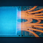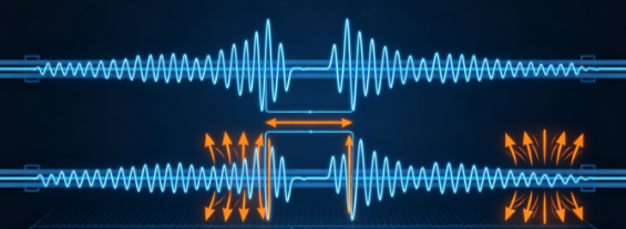
When a differential pair suddenly crosses a discontinuity in its reference plane—for example, a split plane, a thermal pad clearance, a power-island boundary, or a large void in an internal reference layer—the electromagnetic field around the transmission path can change significantly. This discontinuity can increase coupling to adjacent traces and degrade overall signal integrity.
The problem is not simply that the return current has been “disconnected.” Instead, the current must redistribute around the discontinuity, changing the return path, local impedance, field distribution, and mode balance of the differential pair. If the two conductors experience different electromagnetic environments, part of the differential-mode energy can be converted into common-mode energy, increasing the potential for PCB crosstalk and EMI.
For high-speed interfaces such as PCIe, the effect should be evaluated using the actual stackup, trace geometry, dielectric thickness, signal rise time, plane structure, and neighboring networks rather than relying on a single universal spacing or offset-length rule.
Reference Plane Misalignment Is an Impedance and Field-Distribution Problem
A reference plane discontinuity does not necessarily eliminate the signal’s return path. Instead, it forces the high-frequency return current to redistribute around the opening or offset region. This increases the effective loop area and can introduce additional inductive impedance.
For a rapidly changing signal, the induced voltage associated with parasitic inductance can be conceptually described by:
[V=L\frac{di}{dt}]
where L represents the effective loop inductance and di/dt represents the rate of current change.
The more important issue for a differential pair is often return path asymmetry. If one conductor is closer to the edge of a plane opening while the other is farther away, the two conductors no longer experience identical electromagnetic conditions. This imbalance can cause differential-to-common-mode conversion.
Once common-mode energy increases, more electromagnetic energy can couple into neighboring circuits. Therefore, the observed increase in PCB crosstalk may result from a combination of:
- Return-path discontinuity
- Local impedance variation
- Differential-to-common-mode conversion
- Electric-field redistribution
- Magnetic-field coupling
- Resonance or cavity effects
- Increased coupling to adjacent traces
The severity depends strongly on the relationship between trace width, dielectric thickness, plane geometry, edge rate, and discontinuity dimensions.
Why Dielectric Thickness Changes the Effect
The distance between a high-speed trace and its reference plane strongly influences field confinement. When the dielectric is thin, a larger portion of the electromagnetic field is concentrated close to the trace and reference structure.
A reference-plane opening located directly below the trace can therefore cause a pronounced field redistribution. However, the relationship is not simply “thinner dielectric equals more crosstalk” in every stackup. The actual result depends on trace width, copper thickness, dielectric constant, plane geometry, and neighboring conductors.
For this reason, the final stackup should be evaluated using the actual pressed dielectric thickness rather than only the nominal prepreg specification.
Three Practical Checks for Reference Plane Misalignment
Rather than applying a universal numerical threshold, engineers can use the following checks as an initial PCB design screening method.
1. Short discontinuities
A very short plane offset relative to the trace width may have a limited effect, particularly when the return path can remain close to the signal. However, even a short discontinuity should not automatically be considered harmless for extremely fast edge rates.
As a practical starting point, discontinuities on the order of the trace width should be reviewed, especially for tightly controlled impedance interfaces.
2. Moderate discontinuities
When the discontinuity becomes several times the trace width, the return current may need to travel around a substantially larger region. At this point, engineers should examine the return-path continuity and consider ground stitching structures where appropriate.
Ground stitching vias can help reconnect the return-current environment, but their effectiveness depends on their location, inductance, via geometry, and connection to the relevant reference planes.
3. Large discontinuities
When a plane opening becomes much longer than the trace width and directly overlaps a critical differential route, simply adding stitching vias may not be sufficient.
In such cases, the preferred engineering solution is usually to:
- Move the differential pair away from the opening.
- Restore a continuous reference plane.
- Reroute the pair on another layer.
- Modify the stackup so that an appropriate reference plane is available.
- Reduce the size of the plane void where possible.
The key principle is to eliminate the discontinuity first rather than attempting to compensate for a poor reference structure afterward.
Misalignment vs. Dielectric Thickness
Consider a high-speed differential pair crossing the same reference-plane discontinuity in two different stackups. A thicker dielectric distance between the signal and reference plane can change the electromagnetic field distribution and therefore alter the severity of the discontinuity.
However, dielectric thickness should not be increased simply to reduce crosstalk. A thicker dielectric changes controlled impedance, layer-to-layer coupling, board thickness, via geometry, and potentially mechanical reliability.
For example, a thicker multilayer PCB may introduce additional considerations for:
- BGA solder-joint fatigue
- PCB warpage
- Z-axis thermal expansion
- Via aspect ratio
- Lamination behavior
- Mechanical stress
Therefore, PCB stackup optimization should balance signal integrity, manufacturability, thermal requirements, and mechanical reliability instead of optimizing only one electromagnetic parameter.
Ground Stitching Vias: Useful but Not a Universal Fix
Ground stitching vias are commonly used to maintain return-current continuity around connectors, layer transitions, plane boundaries, and other discontinuities.
Their effectiveness depends on several factors:
- Via-to-trace distance
- Via pitch
- Signal rise time
- Reference-plane separation
- Via inductance
- Ground-plane connectivity
- Nearby plane openings
- Differential-pair geometry
A stitching via located too far from the signal transition may have limited influence because the return current still has to travel through a large loop.
Similarly, adding many vias around an incorrectly routed differential pair does not automatically restore the original electromagnetic environment.
The goal is not simply to maximize the number of ground vias. The goal is to provide a low-inductance return path that remains physically close to the high-frequency current path.
Differential Pair Symmetry Is Critical
A differential pair can tolerate certain environmental variations because its two conductors share much of the same electromagnetic environment. However, this advantage depends on maintaining sufficient symmetry.
If a reference-plane opening is located primarily under one conductor, the pair becomes electrically asymmetric. This can increase:
- Differential impedance imbalance
- Skew
- Common-mode conversion
- Mode-conversion loss
- Coupling to adjacent circuits
- EMI radiation
Therefore, when checking a high-speed differential pair, engineers should inspect the complete cross-section rather than examining only the top routing layer.
This is especially important for multilayer boards where an internal plane on L2, L3, or another layer may contain a power split, copper void, thermal clearance, or anti-pad structure that is not obvious from the top-layer layout.
Common PCB Design Mistakes
Several mistakes frequently create reference-plane problems during high-speed PCB design:
Checking only the signal layer
A differential pair may appear correctly routed on the top layer while the reference plane underneath contains a large clearance or split.
Assuming differential routing eliminates return-path requirements
Differential signaling reduces sensitivity to some external noise sources, but it does not eliminate the need for a suitable reference structure.
Using a large copper void for thermal or power reasons without SI review
Thermal pads and power islands can unintentionally create discontinuities underneath high-speed traces.
Adding stitching vias after routing is complete
Stitching vias should be considered as part of the return-path architecture, not simply as a late-stage repair.
Relying only on ideal simulation models
Some simulation setups assume an ideal continuous reference plane. If the actual plane opening, copper clearance, via structure, and stackup are not included in the model, the simulation may not reproduce the real board behavior.
How to Verify Reference Plane Problems
A reliable verification process should combine physical inspection and electrical measurements.
Start with the actual PCB stackup, including:
- Pressed dielectric thickness
- Copper thickness
- Trace width and spacing
- Reference-plane geometry
- Plane openings
- Via structures
- Surface finish
- Neighboring signal layers
Then perform a return-path review for all critical differential interfaces.
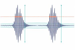
For particularly sensitive designs, electromagnetic simulation can be used to evaluate field distribution, impedance discontinuities, and differential-to-common-mode conversion. TDR can help identify physical impedance discontinuities, while S-parameter measurements can provide additional information about insertion loss and mode conversion.
Eye-diagram testing can then be used at the system level to determine whether the physical discontinuity produces a measurable impact on the actual interface.
The measurement setup itself must also be controlled. Connector launches, probe loading, cable quality, fixture design, and calibration can all affect high-speed measurements.
A Practical CAM Review Workflow
Before releasing a high-speed board to manufacturing, PCB manufacturing data should be checked together with the actual stackup.
A practical review workflow is:
- Identify all high-speed differential pairs.
- Determine the intended reference plane for each routing segment.
- Check whether any plane split or copper void overlaps the pair.
- Measure the discontinuity relative to trace width and dielectric thickness.
- Inspect differential-pair symmetry around the discontinuity.
- Check nearby ground stitching vias and their connection to the reference plane.
- Review layer transitions and via anti-pads.
- Simulate critical discontinuities when necessary.
- Validate the final design through prototype measurements.
- Feed measurement results back into the manufacturing design rules.
The screening criteria should be based on the interface’s actual rise time, stackup, geometry, and supplier capability rather than a single universal “safe” offset length.
Kingda’s Approach to High-Speed PCB Design
At Kingda, high-speed PCB design reviews can integrate stackup analysis, impedance control, return-path inspection, DFM review, and prototype validation into the manufacturing process.
For critical differential interfaces, the objective is not simply to route two traces with the correct spacing. The complete electromagnetic environment—including the reference plane, return path, layer transitions, vias, copper geometry, and neighboring networks—must be considered.
By identifying reference-plane discontinuities during the design and CAM review stages, engineers can reduce avoidable PCB crosstalk, improve signal integrity, and minimize costly redesigns during prototype or mass production.