The cost of correcting impedance problems increases rapidly as a PCB project moves from prototyping to mass production. During the prototype stage, dielectric-related impedance issues can often be addressed by modifying the stackup or material selection. Once a product enters volume production, however, an impedance failure caused by dielectric variation can result in expensive redesigns, material waste, production delays, and schedule disruption.
For this reason, PCB Dielectric Design should be incorporated into the DFM (Design for Manufacturability) review from the beginning of a multilayer PCB project. Evaluating dielectric materials, stackup construction, copper distribution, and impedance test structures early can help engineers identify manufacturing risks before fabrication and reduce the probability of costly rework.
1. Review the PCB Stackup and Dielectric Materials During DFM
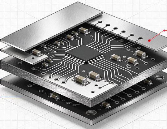
The first step in a dielectric-focused DFM review is to verify the complete PCB Stackup. Engineers should confirm the layer sequence, core materials, prepreg (PP) specifications, copper thickness, dielectric thickness, and the material parameters used for impedance calculations.
Important parameters may include:
- Dielectric material and manufacturer part number
- Resin content of prepreg
- Nominal dielectric thickness
- Finished dielectric thickness after lamination
- Dk (dielectric constant)
- Df (dissipation factor)
- Test frequency used for Dk/Df characterization
- Copper thickness
- Target single-ended and differential impedance
Mixing different Dielectric Material systems without accounting for their electrical characteristics can make the effective dielectric constant difficult to predict. Similarly, stacking multiple prepreg sheets can introduce thickness variation because the final thickness depends on resin content, copper pattern, lamination pressure, temperature, and other process conditions.
For high-speed designs, engineers should also consider the frequency and temperature dependence of Dk and Df. Using a single nominal Dk value without understanding how the material behaves across the operating frequency range can lead to discrepancies between simulated and measured impedance.
A robust DFM review should therefore include the complete stackup and material specification together with the impedance calculation or simulation report. Checking only trace width, spacing, and drill size is not sufficient for impedance-controlled multilayer PCBs.
2. Copper Distribution and Its Effect on Dielectric Thickness
Copper distribution is another important DFM consideration because it can affect the final dielectric thickness after lamination.
Large copper areas, isolated copper features, and significant differences in copper density between adjacent regions can change how resin flows during lamination. Resin tends to flow into areas with less copper, while dense copper regions can restrict resin movement. As a result, the finished dielectric thickness may vary across the PCB.
Because controlled impedance depends on the relationship between trace geometry, copper thickness, dielectric thickness, and dielectric properties, local variations in the dielectric layer can produce impedance variation across the same board.
Designers can reduce this risk by improving copper balance during layout and panelization. Common approaches include:
- Maintaining a more uniform copper distribution across layers
- Using copper balancing features where appropriate
- Avoiding excessively large copper-free areas
- Reviewing large isolated copper regions
- Considering copper thieving or pattern balancing when appropriate for the manufacturing process
- Maintaining continuous reference planes beneath critical high-speed traces
For high-speed differential pairs and other impedance-controlled traces, the reference plane should remain as continuous as possible. Unnecessary openings or slots beneath a signal trace can interrupt the return-current path and increase electromagnetic coupling.
Reference-plane openings can also change the local electromagnetic environment of the transmission line. Therefore, copper distribution and reference-plane design should be evaluated together rather than treated as separate layout issues.
3. Design Impedance Test Structures Correctly
A properly designed impedance test structure is essential for meaningful Impedance Testing. If the test coupon does not accurately represent the product’s actual transmission-line structure, the measured result may not provide a reliable indication of the PCB’s impedance performance.
During DFM review, engineers should verify that the impedance coupon uses the same:
- Layer structure
- Dielectric construction
- Copper thickness
- Trace geometry
- Reference-plane configuration
- Surface-finish conditions where relevant
For example, an inner-layer stripline should be represented by an appropriate test structure rather than using a surface microstrip coupon that has a fundamentally different electromagnetic structure.
The test trace also needs sufficient length for the selected TDR measurement method and equipment. An excessively short structure may make measurement accuracy more difficult, particularly when the transition and launch effects occupy a significant portion of the measured waveform.
Coupon placement should also be considered. Depending on the manufacturing panel and specification, coupons may be positioned at locations that help evaluate variation associated with panel edges, center regions, or different production areas.
The objective is not simply to obtain an impedance number. The test structure should be designed so that the measured value can be meaningfully correlated with the impedance-controlled traces on the actual PCB.
4. Standardize Dielectric and Impedance Requirements in Manufacturing Documents
A common source of manufacturing ambiguity is an incomplete impedance specification. Simply stating “50 Ω impedance control” does not provide enough information for a manufacturer to reproduce the intended electrical structure.
A complete specification should define the relevant Dielectric Material and electrical requirements, including, where applicable:
- Material family or specific material designation
- Dk and the corresponding test frequency
- Core and prepreg specifications
- Target dielectric thickness
- Required copper thickness
- Single-ended impedance target and tolerance
- Differential impedance target and tolerance
- Controlled-impedance layer or net information
- Impedance calculation or simulation requirements
- Impedance Testing method
- TDR measurement requirements
- Applicable acceptance criteria
Material requirements should not depend on informal communication between engineering and production teams. They should be documented in the fabrication drawing, stackup documentation, impedance table, or other controlled manufacturing documents.
This approach reduces the possibility of material substitution or incorrect interpretation during procurement and production.
At the same time, designers should distinguish between a required material designation and an acceptable material performance range. If equivalent materials are permitted, their electrical, thermal, mechanical, and processing characteristics should be reviewed before substitution.
5. Close the Loop During Prototype Production
A DFM review should not end when the design is released for fabrication. Prototype production provides an opportunity to validate whether the selected PCB Stackup, Dielectric Material, and impedance model accurately represent the finished board.
After prototype fabrication, the manufacturer can perform Impedance Testing using an appropriate TDR-based method and compare the measured results with the design targets and simulation values.
If a significant deviation is identified, engineers should investigate possible causes rather than immediately changing trace width. Potential contributors include:
- Actual dielectric thickness after lamination
- Material Dk variation
- Resin content and resin flow
- Copper thickness variation
- Trace etching variation
- Stackup construction
- Surface finish effects
- Test-coupon structure
- Measurement setup and calibration
For high-speed designs, the difference between nominal material data and actual manufactured characteristics can be particularly important. If necessary, measured data from the prototype can be used to refine the stackup model and improve subsequent production revisions.
Resolving these issues during prototype builds is generally more manageable than discovering them after volume production has started.
6. Consider Dielectric Thickness Tolerance in Impedance Design
Dielectric thickness is one of the most influential physical parameters in controlled-impedance structures. Even when the nominal stackup is correct, the finished thickness can vary because of material tolerance and lamination conditions.
Therefore, impedance calculations should not rely exclusively on nominal values. Where the application requires tight impedance control, engineers should evaluate reasonable manufacturing tolerances for dielectric thickness, copper thickness, trace width, and etching.
A tolerance-aware design can help determine whether the specified impedance target remains achievable across normal manufacturing variation.
For example, when designing a 50 Ω single-ended or 100 Ω differential interface, the objective should be to create sufficient manufacturing margin rather than selecting a geometry that works only at one idealized stackup value.
7. High-Speed PCB Design Requires Special Attention to Dielectric Properties
For high-speed interfaces, PCB Dielectric Design becomes closely connected to signal integrity.
The dielectric material influences:
- Characteristic impedance
- Propagation delay
- Insertion loss
- Dielectric loss
- Crosstalk behavior
- Signal rise-time performance
- High-frequency attenuation
The nominal Dk value alone may not fully describe high-speed transmission behavior. Different measurement methods and frequencies can produce different reported values, so the Dk data used in simulation should be appropriate for the intended application.
For demanding high-speed interfaces, designers should evaluate the complete transmission-line structure, including trace geometry, reference-plane spacing, copper roughness, dielectric loss, and material dispersion.
The PCB Stackup should therefore be developed together with signal-integrity requirements rather than being selected independently after routing is complete.
8. Avoid Common Dielectric-Related DFM Mistakes
Several design practices can increase the risk of impedance problems:
| Common Issue | Potential Effect | Recommended DFM Approach |
|---|---|---|
| Incomplete material specification | Incorrect material selection | Define the required dielectric system clearly |
| Excessive copper-density variation | Uneven resin flow and dielectric thickness | Improve copper balance |
| Inappropriate impedance coupon | Unrepresentative measurement | Match coupon structure to actual transmission lines |
| Nominal Dk used without frequency context | Simulation-to-measurement deviation | Use application-relevant material data |
| Large reference-plane openings | Disrupted return path | Maintain continuous reference planes where required |
| Uncontrolled material substitution | Impedance and reliability changes | Review electrical and process equivalence |
| No stackup tolerance analysis | Reduced manufacturing margin | Include realistic material and geometry tolerances |
| Incomplete impedance documentation | Production interpretation errors | Define targets, tolerances, materials, and test methods |
9. Integrate Dielectric Evaluation into the Complete DFM Workflow
The most effective approach is to treat dielectric analysis as part of the complete DFM workflow rather than as a separate activity performed only after impedance problems occur.
A practical review can include the following sequence:
- Review the required electrical interfaces and impedance targets.
- Define the PCB Stackup and reference-plane structure.
- Select appropriate Dielectric Material systems.
- Verify Dk/Df data and applicable frequency ranges.
- Evaluate dielectric and copper thickness tolerances.
- Review copper distribution and lamination-related risks.
- Check trace geometry and impedance calculations.
- Review impedance coupon design.
- Document manufacturing and testing requirements.
- Validate the design through prototype Impedance Testing.
- Compare measured data with simulation and update the model when necessary.
- Freeze the validated stackup before volume production.
This closed-loop approach helps connect PCB design, fabrication engineering, material selection, and quality control.
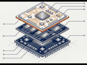
10. Kingda PCB Dielectric and Impedance DFM Support
Kingda can support customers in reviewing multilayer PCB designs with attention to manufacturability, stackup construction, material selection, impedance requirements, and production considerations.
For impedance-controlled designs, the engineering review can focus on the relationship between PCB Stackup, Dielectric Material, copper geometry, transmission-line structure, and manufacturing tolerances.
A well-defined DFM process helps identify potential dielectric and impedance risks before fabrication, reducing the possibility that a design reaches mass production with unresolved stackup or impedance issues.
Conclusion
Reliable impedance control begins with the dielectric system, not simply with trace width adjustment. The PCB Stackup, Dielectric Material, copper distribution, reference-plane structure, manufacturing tolerances, and impedance test coupon all contribute to the final electrical performance of a multilayer PCB.
By integrating PCB Dielectric Design and Impedance Testing into the DFM process, engineers can identify material and manufacturing risks earlier, improve the correlation between simulation and production results, and reduce the likelihood of costly redesigns during mass production.
For high-speed and impedance-controlled multilayer boards, a validated stackup and clearly documented dielectric requirements provide a much stronger foundation for stable manufacturing and reliable signal integrity.