PCB Edge Plating: EMI Shielding and Grounding
Most of a circuit board is designed on its faces, with the edges treated as a cutting line. Edge plating changes that by putting conductor on the edge itself, connecting the outer layers and sometimes the inner ground planes around the perimeter of the board. It is a small feature that solves several problems at once, and it is one of the few processes where the board outline becomes an electrical parameter.
What Edge Plating Is
Edge plating is a conductive layer deposited on the routed edge of a board, which links the copper on the top and bottom surfaces and any inner layers that are exposed at that edge. The connection is continuous along the plated section rather than through discrete holes.
It differs from a castellation, which is a plated half hole formed at the board edge to allow a module to be soldered down to a carrier board. A castellation is a connection point, while edge plating is usually a continuous shield or ground connection along a length of the outline.
Why It Is Used
The first reason is shielding. A plated edge, combined with a shielded cover, closes the enclosure around the electronics and stops radiation from escaping through the gap between the board and the housing. That matters for radio modules and for any product with a tight emission limit.
The second is grounding. Connecting the top and bottom ground planes at the perimeter shortens the return path for currents that would otherwise travel to the nearest via, and it reduces the parallel plate resonance that forms between two large planes. Both effects improve EMC performance without adding components.
How the Process Works
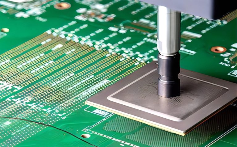
Edge plating requires the outline to be formed before plating, which means the board is routed or milled to its final shape while the panel is still intact, and the plated edge is then connected to the copper pattern and passed through the plating line.
The edge must be conductive before plating, which is why the process starts with a metallisation step on the milled edge. Plating thickness is controlled in the same bath as the hole plating, and the requirements for both are usually specified together. The chemistry involved is described in electroplating additives for PCB.
Board Outline Tolerance
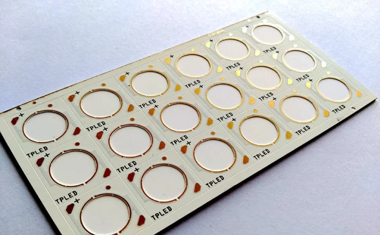
Because the plating follows the milled outline, the accuracy of that outline becomes part of the electrical design. A variation in the routing position changes the width of the plated band and, where the edge is meant to contact a housing, changes the mechanical fit.
These considerations make the outline a controlled feature rather than a mechanical afterthought, and the tolerances that apply are discussed in board outline and mounting design. Where a gasket or a spring finger will contact the plated edge, the tolerance has to account for the compression of the contact as well as for the routing.
Design Rules
The plated edge needs a defined width, typically a fraction of a millimetre, and a clear region inside it on the outer layers so that the plating does not accidentally contact signal copper. Ground copper should overlap the plated band deliberately, with a solid connection rather than a thin neck.
Inner layers that meet the plated edge must be intended to do so. A plane that reaches the edge will be shorted to the plating, which is usually the objective, but a signal layer that happens to reach the outline will be shorted as well. The layer drawing must therefore define which inner layers are exposed at the edge.
Castellations and Module Edges
A castellated edge is the other common use of edge plating. A small module is built as part of a panel, and its edge is drilled with half holes that are plated and then cut through, leaving a solderable half cylinder at the edge of the finished module.
The module can then be soldered onto a carrier board like a surface mount component, with the joint formed against the castellation rather than against a pad. The advantage is a strong, inspectable joint and a low profile, and the requirement is precise alignment between the drilled holes and the routed edge.
Plating Thickness and Quality
Plating thickness on an edge is specified for the same reasons as in a hole: it determines the current capacity and the durability of the connection. Copper of twenty five micrometres is a common specification, with more where the edge carries significant current or where it will be handled repeatedly.
Adhesion is the quality issue. The plated layer has to bond to the laminate edge, which is a cut surface rather than a drilled wall, and a poor bond shows up as blistering or flaking after thermal cycling. Inspection by microsection on a sample confirms the thickness and the bond.
Working with the Housing
EMI shielding with a plated edge only works if the plating actually contacts the housing. A spring finger, a conductive gasket or a machined step in the enclosure has to press against the plated band along its whole length, and the contact has to survive the tolerance stack of the board, the housing and the assembly screws.
The design should therefore state where the contact is made and how much compression is available. A plated edge that meets a painted surface provides no connection at all, and one that contacts only at a few points behaves like a set of discrete vias rather than a continuous shield. Both faults are mechanical, and both are invisible in an electrical schematic, which is why they belong in the drawing review.
Applications
Radio modules use edge plating to form a shielded enclosure in combination with a metal can. Automotive and industrial boards use it to improve emissions performance where the board is close to the housing. Test and measurement equipment uses it where a defined ground reference is needed at the perimeter.
Castellations appear in modules of every kind, from power converters to radio subassemblies, because they allow a fully tested module to be treated as a component. The shielding aspects overlap with the general techniques described in EMI suppression design principles.
Cost and Sourcing
Edge plating adds cost because the outline is formed earlier in the process, the plating step is longer and the handling requirements are stricter. Castellations add a drilling step and a tighter tolerance between the drill pattern and the outline.
The premium is modest compared with the alternative of a separate shield can and its assembly operation, which is why the process is common in high volume radio products. The supplier should be asked about the plating thickness tolerance, the outline tolerance and the microsection evidence, since all three determine whether the feature works in production.
FAQ
Can any board have a plated edge? Most can, provided the outline allows the plating to be connected to the copper pattern. Very thin boards and unusual shapes may need special handling.
Does edge plating replace a shield can? It complements one. The plating closes the perimeter, but a can or a shielded housing is still needed to cover the top and bottom.
How is the plated edge connected to ground? Through overlapping copper on the outer layers and through the inner layers that are deliberately exposed at the edge. The overlap should be generous rather than a thin bridge.