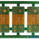
Embedded Resistor: Design Rules and Process Limits
An embedded resistor is a resistive layer inside the board, patterned into individual elements and connected to the rest of the circuit by vias. It replaces a discrete part with a structure that has no solder joint and no placement, and it is used where the number of passive components or the available area has become the limiting factor rather than the electrical requirement.
The Two Approaches
The first approach uses a resistive foil laminated into the stack. The foil is a thin alloy layer with a defined sheet resistance, and the resistor is formed by etching a pattern whose length and width set the value.
The second approach prints a resistive ink onto an inner layer and cures it. The printing process allows a wider range of values without changing the laminate, and the tolerance is generally wider than for a foil.
Both are patterned in the same way as copper, and both are connected with vias in the same way as any other inner layer feature. The choice between them is a trade of tolerance, value range, cost and the number of suppliers.
Sheet Resistance and Geometry
Sheet resistance is the resistance of a square of the material, and it does not depend on the size of the square. The value of a resistor is the sheet resistance multiplied by the number of squares, which is the length divided by the width.
The consequence is that the value is set by geometry rather than by area. A resistor of the same value can be long and narrow or short and wide, and the choice is usually made for the space that is available rather than for an electrical reason.
The number of squares is limited in practice. A very long narrow resistor occupies a large area, while a very short wide one approaches the tolerance limit of the etching process, since a small dimension is harder to hold than a large one.

Tolerance and Trimming
The as etched tolerance of an embedded resistor is wider than that of a discrete part, typically several percent for a foil and more for a printed layer. The variation comes from the material, the etching and the thickness.
Trimming closes part of that gap. A laser cuts a kerf in the element and increases its resistance in a controlled way, and the measurement is made during the cut. The trim is usually applied after the layer has been processed, which means the value is set with the finished geometry.
Active trimming measures each element and cuts until the target is reached, while passive trimming uses the same cut for every element and relies on the uniformity of the material. Active trimming gives a tighter result and takes longer, so it is applied to the elements that need it.
Design Rules
The resistive layer needs a defined area for each element, and that area comes out of the available space on the layer. Dense embedded passives therefore increase the pressure on the routing rather than relieving it unless the resistor replaces a part that would otherwise be on the surface.
The element should not be placed under a heavy mechanical stress. A region that flexes, a press fit hole and a connector footprint are all places where a brittle resistive layer can crack.
The connection to the element is made with vias, and the vias should be placed so that the current distribution is uniform. A via at one corner of a wide element creates a current concentration that changes the effective number of squares.
Layer Count and Cost
Adding a resistive layer adds at least one layer to the stack, and often two if the design wants the resistors on both sides of a plane. The extra layers cost more than the parts they replace unless the part count or the surface area is the driving constraint.
The cost also includes the yield. A board with embedded passives cannot have a single element repaired, so an element that fails a measurement after lamination takes the whole board with it.
The economic case is strongest on a board with a large number of identical resistors in a small area, such as a termination array or a filter bank, where the area saved on the surface is worth more than the extra layer.
Testing and Verification
Embedded resistors are tested through their nets, either at the final test or with a dedicated coupon on the panel. The resistance of an element can be measured across two test points, and the measurement has to allow for the resistance of the traces that lead to them.
The coupon is the more useful measurement, because it isolates the material from the routing. A coupon that measures outside the specification points at the material or the process, while an individual element that is out of specification with a good coupon points at the geometry.
The trimming record is part of the quality evidence. A trimmed element should have its value recorded, and the record should show whether the trim reached the target or whether it was stopped at a limit.
Reliability
The failure modes of an embedded resistor are different from those of a discrete part. There is no solder joint to crack, but there is a layer that can crack under thermal cycling, a material that can change value with temperature and a via that can be affected by the expansion of the surrounding laminate.
The temperature coefficient of the material is an important specification. A foil with a low coefficient holds its value over a wide temperature range, while a printed layer may drift enough to matter for a circuit that depends on the ratio of two resistors.
The long term stability should be supported by data from the supplier rather than by assumption. A drift of a few percent over the life of a product is acceptable for a pull up resistor and unacceptable for a precision divider.
Where It Makes Sense
The cases that justify embedded resistors are a termination array, a filter bank, a divider that has to track over temperature and any design where a large number of identical passive components has become the bottleneck in placement or in board area.
The cases that do not justify it are a design with a handful of resistors, a design that needs a wide range of values and a design that expects to be reworked repeatedly during development.
The decision should be made early, because the electrical design, the stackup and the test strategy all depend on it. A project that decides to embed resistors after the layout is complete will find that the gains are much smaller than the brochure suggests.
Practical Rules
Choose the material for the tolerance and the temperature coefficient, size the element by the number of squares, and reserve trimming for the values that need it. Keep the elements away from mechanical stress.
Record the material, the trimming results and the coupon data with the build records and the layer count selection, and review the laminate properties and the embedded capacitor design when the stackup is being planned.
FAQ
How is the value of an embedded resistor set? By geometry. The sheet resistance of the material is fixed, and the value is the number of squares, which is the length divided by the width of the element.
What tolerance can be achieved? Wider than a discrete part as etched, typically several percent for a foil. Laser trimming after processing brings individual elements closer to target.
Why is the economic case narrow? The layer costs more than the parts it replaces unless board area or part count is the constraint, and a failed element cannot be repaired after lamination.