
Copper Balance Design For Multilayer Panels
Copper balance is the extent to which the amount and the distribution of copper on each layer of a board match the layers around it. An unbalanced design distorts during lamination and produces boards that are warped, that vary in thickness, or that fail to sit flat in an assembly fixture.
The rule is easy to state and hard to apply, because a real design has dense areas and empty areas by nature. The aim is not perfect symmetry but enough symmetry that the fabricator can build the panel without adding dummy copper to every empty region.
Why Balance Matters
During lamination the resin flows to fill the space around the copper, and the amount of resin that has to move depends on how much copper is present. A layer with little copper needs a lot of resin to fill the gap, while a layer with a large ground plane needs very little, so the two behave differently under the same pressure.
The consequence is that the finished thickness and the internal stress vary from point to point. A panel that cools with an uneven stress distribution bows, and the bow survives into the finished board because the copper is bonded to the resin.
Warpage And Its Causes
Warpage is measured as the deviation of a board from flat, usually expressed as a percentage of the diagonal length. The usual limit for a surface mount board is 0.75 percent, and it is tighter for a board carrying fine pitch parts or a large ball grid array.
The causes are unbalanced copper, an asymmetric stackup and a lamination cycle that cools unevenly. Of the three, unbalanced copper is the one the designer controls directly, and it is usually the largest single contributor on a mixed design. The dimensional behaviour behind this is described under PCB dimensional stability and expansion.
Resin Flow And Thickness Variation
Resin flow is the movement of the partly cured resin during lamination, and it is what fills the space between conductors. Where copper is dense there is little room for resin and the dielectric layer thins, which changes the impedance of the traces above it.
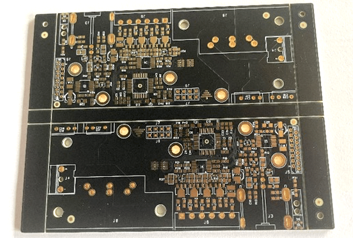
Impedance controlled boards are therefore sensitive to copper distribution even when the nominal stackup is correct. A trace above a dense area can have a lower impedance than the same trace above an empty area, and the coupon may not reveal it because the coupon has its own distribution. How that affects impedance control is described under PCB routing and microstrip or stripline.
Measuring Copper Distribution
The practical measure is the percentage of copper on each layer, counted over the panel area, and the difference between adjacent layers or between the two halves of a symmetric pair. A common guideline is to keep the difference between the two sides of the stack below about 20 percent.
More refined checks look at the distribution across the panel as well as between layers. A layer that is 50 percent copper overall but concentrated in one corner will still cause problems, so local balance matters as much as the average figure.
Adding Balancing Features
Where the difference is too large, the usual answer is to add copper that carries no signal. A ground pour on a sparse layer, a grid of isolated pads, or a strip of copper in the panel border all raise the copper percentage without changing the circuit.
The added copper has to be considered as part of the electrical design. A floating plane can become an antenna, and a pour connected to a net must not create an unintended path. Where copper is added purely for mechanical reasons it is usually left isolated and made small enough not to resonate.
Working With The Fabricator
Balance is finally a matter for the fabricator, who knows the press, the prepreg and the flow characteristics of the material. Sending the layer images early, with the copper percentage for each layer, allows the fabricator to comment before the data is released rather than after the first panel warps.
The agreed balance should be recorded with the stackup, so that a later revision does not silently change the copper distribution. How the stackup and its constraints are documented is described under layer stackup from one to eight layers.
Process Control and Verification
On a design of this kind, resin flow is the item that decides how the rest of the board is arranged. Keeping a sample from the panel turns a dispute into a measurement, because the same coupon can be re-examined by both parties without rebuilding the batch. Reviewing the design before the data is released is cheaper than correcting it after the panel is in the tank, because every step downstream inherits the decision made at the front end.
Documenting the assumption is part of the design work, and a short note on the drawing prevents a question that would otherwise arrive a day later and cost a day of schedule. The process window is set by the narrowest step in the flow, so an improvement anywhere else shows up as margin rather than as yield until that step is addressed.
A short note on the drawing about handling, storage or packaging is often worth more than an extra decimal place on a tolerance. Where a value sits close to a process limit, the drawing should say so, since the shop can then open the process window rather than working to a nominal figure that carries no tolerance.
Process Control and Verification
On a design of this kind, resin flow is the item that decides how the rest of the board is arranged. Keeping a sample from the panel turns a dispute into a measurement, because the same coupon can be re-examined by both parties without rebuilding the batch. Reviewing the design before the data is released is cheaper than correcting it after the panel is in the tank, because every step downstream inherits the decision made at the front end.
Documenting the assumption is part of the design work, and a short note on the drawing prevents a question that would otherwise arrive a day later and cost a day of schedule.
Process Control and Verification
On a design of this kind, resin flow is the item that decides how the rest of the board is arranged. Keeping a sample from the panel turns a dispute into a measurement, because the same coupon can be re-examined by both parties without rebuilding the batch. Reviewing the design before the data is released is cheaper than correcting it after the panel is in the tank, because every step downstream inherits the decision made at the front end.
A first article check confirms that the process and the drawing agree on the points listed above, and that the coupon data supports the values used in the design.

Where a measurement falls outside the expected window, the sample is retained so that the cause can be established before the balance of the batch is released.
FAQ
Can warpage be corrected after the board is made? Not reliably. A warped board can sometimes be flattened by baking under weight, but the internal stress remains and the board tends to return to its original shape.
Does a ground plane on both sides always solve balance? It helps a great deal because the two planes are usually similar, but the other layers still matter. A pair of planes with very different signal layers beside them can still be unbalanced.
How much copper difference is acceptable? Around 20 percent between the two sides of a stack is a common guideline. Tighter limits apply to thin boards, large panels and fine pitch assemblies.