Fabrication Drawing Checklist for PCB Production
A fabrication drawing is the document that turns a set of Gerber files into a defined product. The data describes where copper goes; the drawing describes how thick, how flat, how clean and how it is to be verified. When the drawing is incomplete, the fabricator supplies its own defaults, and those defaults are rarely what the designer assumed.
Why the Drawing Exists
The artwork and the fabrication note serve different purposes. One carries the physical geometry, the other carries the electrical and mechanical expectations, the acceptable alternatives and the exceptions to the standard process. Neither is complete without the other.
Almost every requirement has an exception, and the note is where those exceptions are recorded. Writing them down protects both sides, because a fabricator that has to interpret an ambiguous requirement will choose the interpretation that is easiest to manufacture.
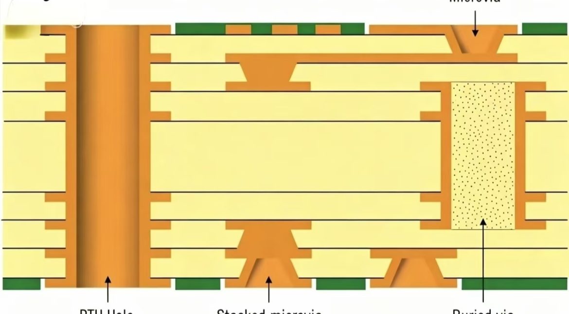
<img src="https://www.gopcba.com/wp-content/uploads/2026/04/Solar-Inverter-Systems.jpg" alt="Fabrication drawing notes beside a PCB stackup diagram” />
Standards and Class of Build
The drawing normally names the standards that apply. For rigid boards the usual callout is IPC Class 2 of the current revision of the rigid specification, with dimensions interpreted according to the applicable drawing standard and with the artwork reproduced at one to one scale.
Naming a class is not a formality. Class 2 defines acceptance criteria for annular ring, plating thickness, hole quality and cosmetic defects, and it decides what the inspector will reject. Flexible circuits follow their own specification, and a board that mixes rigid and flexible sections needs both.
Material Callouts
Material is specified by performance rather than by trade name wherever possible: a glass transition temperature, a flammability rating, a halogen-free requirement and compliance with the restriction on hazardous substances. Equivalent materials are usually allowed, subject to approval.
Copper foil thickness belongs in the stackup drawing rather than in the general note, because it differs by layer and it determines the impedance of every controlled trace. The laminate and prepreg types should be listed with their dielectric thickness so the stackup can be reproduced exactly.

Flatness, Bow and Twist
Flatness is expressed as a maximum deviation per unit length, commonly 0.025 mm per mm, measured before or after assembly according to the agreed method. It matters most for thin boards and for large panels that will be populated with fine pitch parts.
Test method matters as much as the number. Referencing a specific section of the standard test manual removes the argument about how the measurement was taken, and controlling dimensional stability in the stackup is what makes the requirement achievable.
Etch Geometry and Dimensional Tolerance
Trace width is defined with a tolerance and a measurement basis. A common requirement is that the finished width does not deviate by more than a fixed dimension or a percentage of the artwork, whichever is smaller, with the width measured at the base of the conductor.
Minimum line width and minimum spacing are stated for outer and inner layers separately, because the processes differ. Positional tolerance for drilled features is also stated, typically as a maximum deviation from the true position given in the CAD data.
Vias, Holes and Plating
Plating requirements define copper thickness in the barrel and the acceptability of the deposit. A continuous electrolytic copper layer with a stated minimum thickness is the normal callout, and the hole size is measured after plating rather than before.
The drill chart should carry the finished hole sizes and their tolerances, and vias that will be filled or capped need their own note. Where a via sits under a component, the filling and the plating process have to be specified together so the surface finishes flat.
Surface Finish Selection
The drawing should select one finish and cite the specification that governs it, including the layer thicknesses for each metal. A nickel and gold finish is defined with its nickel thickness, its gold thickness and, where a palladium layer is used, the thickness of that as well.
Where the panel has different requirements on different areas, selective plating is stated with the areas defined by layer or by reference designator, so that the plated region is unambiguous and the cost of gold is limited to where it is needed.
Solder Mask, Legend and Marking
Solder mask is specified by the applicable mask standard, by colour, by thickness range and by the requirement that no traces are exposed. Mask on bare copper with mask over bare copper construction is the common callout on modern boards.
Legend requirements cover ink type, colour, minimum line width and the rule that print must never contact exposed metal. Supplier identification, date code and any added marking are placed on a nominated side so they do not interfere with assembly or with the appearance of the product.
Testing, Impedance and Packaging
Electrical test is specified as a percentage, usually one hundred percent, against the netlist with a defined test standard and class. Impedance requirements are stated per structure with a tolerance, and the drawing should say how much latitude the fabricator has to adjust geometry to hit the target.
Delivery conditions complete the package: a certificate of compliance with each shipment, sample coupons for destructive analysis, identification of scrap panels and packaging that protects the boards in transit. Specifying all of this once is far cheaper than discovering a gap after the first shipment arrives.
Panelisation and Delivery Format
The way boards are arranged on a production panel affects cost, flatness and assembly. The drawing should state the panel size, the number of circuits, the spacing between them and the type of tabs or breakaway features to be used, because the fabricator will otherwise choose a layout that suits its own process.
Delivery format matters too. Whether the supplier ships panels or singulated boards, and which layer of the file set is authoritative, should be stated so that the delivered article matches what the assembly house expects to receive.
Handling Deviations and Substitutions
A good note tells the fabricator what to do when something cannot be met, rather than leaving it to chance. A requirement that any deviation be reported before shipment, with the proposed alternative and its effect, turns a potential surprise into a decision the designer can still influence.
Substitution rules belong in the same section. If an equivalent laminate may be used, say under what conditions; if it may not, say that as well. Ambiguity on this point is what produces a board that passes inspection and then behaves differently in the field.
Reviewing the Drawing Before Release
The final check is a read-through against the design itself. Confirm that the layer count, the finished thickness, the copper weights and the impedance targets match the layout, and that the finishes named on the drawing are the same ones the assembly process assumes.
It is also worth confirming that the drawing and the file set agree on the board outline, the tooling holes and the marking. Most disputes between a designer and a fabricator come from a detail that appears in one document and contradicts the other.
FAQ
Is a fabrication drawing mandatory? For simple boards the Gerber data plus a short note may be enough. Once there are controlled impedance traces, special finishes or tight flatness requirements, a drawing is the only way to state them unambiguously.
What is the most commonly omitted item? Impedance requirements and the latitude allowed to adjust geometry. Without those, the fabricator cannot tune the stackup and will either build to its own default or stop and ask.
Should the drawing repeat information in the Gerber files? It should not contradict them. The file set defines geometry; the drawing adds what the files cannot express, such as material, finish, tolerance and test requirements.