Introduction to PCB Manufacturing Process
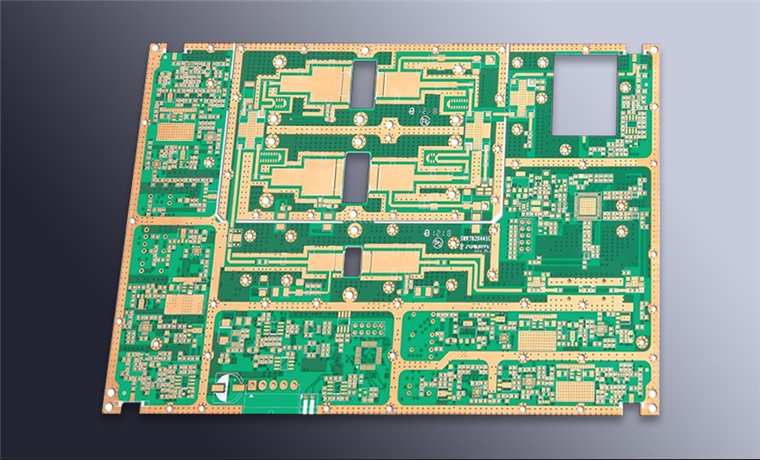
The PCB Manufacturing Process is a highly precise and systematic procedure used to transform raw materials into reliable printed circuit boards for electronic products. With the rapid development of modern electronics, PCB technology continues to evolve to support higher circuit density, faster signal transmission, improved reliability, and more compact product designs.
The production process varies depending on the PCB structure, application requirements, material selection, layer count, and manufacturing technology. Different PCB manufacturers may adopt different equipment and process methods, but the fundamental manufacturing principles remain similar.
Traditional single-sided, double-sided, and multilayer circuit boards are still the foundation of modern PCB Manufacturing. However, advanced technologies such as HDI PCB, fine-line processing, high-frequency materials, and automated inspection systems have significantly improved PCB performance and production capability.
As a professional PCB manufacturer, Kingda provides comprehensive PCB Fabrication solutions, including single-sided PCB, double-sided PCB, and complex Multilayer PCB manufacturing. Through advanced production equipment, experienced engineering teams, and strict quality control systems, Kingda helps customers develop reliable PCB products for various industries.
Overview of PCB Production Process
A complete PCB Production process involves multiple manufacturing stages. Each step requires accurate control of materials, equipment parameters, and production conditions to ensure final PCB performance.
The typical PCB manufacturing workflow includes:
- Engineering review and DFM analysis
- Material preparation and cutting
- Inner layer circuit fabrication
- Layer alignment and lamination
- Drilling and via formation
- Copper plating
- Outer layer circuit fabrication
- Solder mask application
- Silkscreen printing
- Surface Finish processing
- PCB forming
- Electrical testing
- Final inspection and packaging
Every manufacturing stage directly affects PCB reliability, electrical performance, and long-term service life.
Engineering Review and Manufacturing Preparation
Before production begins, PCB manufacturers perform a detailed engineering review of customer design files.
This stage is an essential part of professional PCB Manufacturing because it identifies potential manufacturing problems before fabrication starts.
The engineering team reviews:
- Gerber files
- Drill files
- Layer structure
- Line width and spacing
- Copper thickness requirements
- Impedance control requirements
- Material specifications
- Manufacturing tolerances
Through Design for Manufacturing (DFM) analysis, engineers can optimize the PCB design and reduce possible production risks.
Common issues identified during engineering review include:
- Insufficient spacing between traces
- Difficult routing structures
- Improper hole sizes
- Layer alignment problems
- Manufacturing capability limitations
Early engineering verification improves production efficiency and helps customers reduce unnecessary redesign costs.
PCB Material Preparation and Cutting
The first physical stage of PCB Fabrication is preparing the raw materials.
The most commonly used PCB material is copper-clad laminate (CCL), which consists of a substrate layer and copper foil.
Depending on product requirements, manufacturers may select different materials, including:
- FR-4 materials
- High-frequency laminates
- High-temperature materials
- Flexible PCB materials
- Low-loss dielectric materials
The copper-clad laminate is cut into suitable panel sizes according to production requirements.
Before entering the manufacturing process, materials usually undergo:
- Material inspection
- Baking treatment
- Surface cleaning
- Dimensional verification
Proper material preparation ensures better processing stability during later production stages.
Inner Layer Circuit Fabrication for Multilayer PCB
For a Multilayer PCB, inner layer manufacturing is one of the most critical processes.
The main steps include:
Photoresist Coating
A photosensitive film is applied to the copper surface. This layer allows the circuit image to be transferred accurately.
Circuit Image Transfer
The designed circuit pattern is transferred onto the copper layer through exposure technology.
Developing Process
The exposed areas are developed to reveal the required circuit pattern.
Copper Etching
Unwanted copper is chemically removed, leaving only the designed circuit traces.
Automated Optical Inspection (AOI)
AOI equipment checks the inner layers for defects such as:
- Open circuits
- Short circuits
- Missing traces
- Incorrect patterns
Since inner layer defects are difficult to repair after lamination, strict inspection is essential for high-quality multilayer PCB production.
PCB Lamination Process
After inner layer fabrication, multiple layers are combined through the lamination process.
A multilayer PCB structure usually contains:
- Copper layers
- Prepreg insulation materials
- Core materials
During lamination, heat and pressure are applied to bond all layers together into a complete circuit board.
Important lamination parameters include:
- Temperature control
- Pressure control
- Layer alignment accuracy
- Material compatibility
A reliable lamination process ensures:
- Strong layer bonding
- Stable electrical performance
- Improved mechanical strength
Poor lamination quality may cause problems such as:
- Delamination
- Layer shifting
- Reduced PCB reliability
For advanced electronic applications, precise lamination technology is a key factor in achieving stable PCB Manufacturing results.
PCB Drilling and Via Formation
After lamination, drilling is performed to create holes required for component installation and electrical connections.
Depending on PCB requirements, drilling methods include:
- Mechanical drilling
- Laser drilling
- Microvia drilling
Mechanical drilling is widely used for standard through holes and component mounting holes.
For high-density applications, laser drilling technology is commonly used in HDI PCB manufacturing. Microvias created by laser drilling allow designers to achieve:
- Higher wiring density
- Smaller PCB size
- Improved signal performance
During drilling, manufacturers must carefully control:
- Hole diameter accuracy
- Hole position accuracy
- Drill quality
- Burr removal
High-quality drilling ensures reliable copper plating and stable electrical connections.
Copper Plating Process
After drilling, copper plating is performed to create electrical connections between different PCB layers.
The process generally includes:
Electroless Copper Plating
A thin copper layer is chemically deposited on hole walls to create conductivity.
Electrolytic Copper Plating
Additional copper is deposited to increase thickness and improve reliability.
Copper plating affects:
- Current carrying capability
- Thermal performance
- Mechanical strength
- Electrical reliability
For high-performance PCB applications, accurate copper thickness control is essential.
Kingda applies strict process management during copper plating to ensure consistent PCB quality and long-term reliability.
Outer Layer Circuit Manufacturing
After drilling and plating, the outer circuit layer is produced.
The process includes:
- Circuit image transfer
- Pattern development
- Copper etching
- Circuit inspection
The outer layer determines the final circuit connection structure and directly affects PCB performance.
Manufacturers use advanced inspection methods to verify:
- Circuit accuracy
- Line width
- Spacing
- Surface quality
Reliable outer layer production is essential for successful PCB Assembly and final product performance.
Solder Mask and Silkscreen Printing
The solder mask process protects PCB copper circuits from oxidation and prevents solder bridging during assembly.
The main functions of solder mask include:
- Protecting copper traces
- Improving PCB durability
- Preventing solder defects
- Enhancing electrical insulation
After solder mask application, silkscreen printing is performed.
The silkscreen layer provides:
- Component reference marks
- Polarity symbols
- Product information
- Manufacturing codes
Clear identification improves assembly efficiency and maintenance convenience.
PCB Surface Finish Process
The exposed copper pads require surface protection before component assembly.
This stage is called Surface Finish treatment.
Common surface finish methods include:
HASL
Hot Air Solder Leveling is a traditional and cost-effective finish suitable for many standard applications.
ENIG
Electroless Nickel Immersion Gold provides:
- Flat surface quality
- Excellent solderability
- Strong oxidation resistance
It is widely used in fine-pitch and high-density PCB applications.
Immersion Tin and Immersion Silver
These finishes provide good soldering performance for specific applications.
Hard Gold
Hard gold is commonly used for connector areas requiring high wear resistance.
Selecting the correct Surface Finish depends on:
- PCB application
- Assembly requirements
- Reliability expectations
- Product environment
PCB Forming and Final Processing
After surface treatment, the PCB is processed into the final required shape.
Common forming methods include:
- CNC routing
- V-cut processing
- Punching
The forming process ensures:
- Accurate board dimensions
- Correct outline shape
- Smooth edges
Proper forming quality helps ensure smooth PCB installation during assembly.
PCB Testing and Quality Control
A professional PCB Quality Control system is essential for ensuring PCB reliability.
Before shipment, PCBs undergo multiple inspection procedures.
Common testing methods include:
AOI Inspection
Detects:
- Circuit defects
- Missing traces
- Short circuits
Electrical Testing
Includes:
- Flying probe testing
- Fixture testing
- Continuity testing
Final Quality Inspection
FQC inspection verifies:
- Appearance quality
- Mechanical requirements
- Electrical performance
- Customer specifications
Kingda implements strict PCB Quality Control procedures throughout the manufacturing process to ensure every PCB meets reliability and performance requirements.
Single-Sided PCB Manufacturing Process
Single-sided PCBs contain copper circuits on only one side of the substrate.
The general manufacturing process includes:
Material Cutting → Surface Cleaning → Circuit Formation → Etching → Drilling → Solder Mask → Silkscreen → Surface Finish → Forming → Inspection → Packaging
Single-sided PCBs are commonly used in:
- Consumer electronics
- Simple control products
- Cost-sensitive applications
Although the structure is simple, professional manufacturing control is still required to achieve stable quality.
Double-Sided PCB Manufacturing Process
Double-sided PCBs contain copper layers on both sides and use plated through holes for electrical connection.
The production process includes:
Material Preparation → Drilling → Copper Plating → Circuit Formation → Solder Mask → Silkscreen → Surface Treatment → Testing → Packaging
Compared with single-sided boards, double-sided PCBs provide:
- Higher circuit density
- More design flexibility
- Better electrical performance
They are widely used in industrial equipment, automotive electronics, and communication products.
Multilayer PCB Manufacturing Process
A Multilayer PCB contains multiple conductive layers separated by insulating materials.
The manufacturing process includes:
Inner Layer Fabrication → Inspection → Lamination → Drilling → Copper Plating → Outer Layer Processing → Solder Mask → Surface Finish → Electrical Testing → Final Inspection
Multilayer PCBs provide advantages including:
- Higher routing capacity
- Better signal integrity
- Improved EMI control
- Compact product design
They are widely applied in:
- Medical equipment
- Automotive systems
- Communication devices
- High-speed electronic products
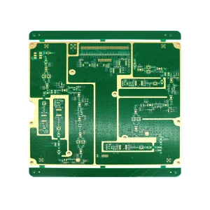
Kingda PCB Manufacturing Capability
With increasing demands for electronic miniaturization and higher performance, PCB manufacturers need advanced technology and strong engineering capabilities.
Kingda provides professional PCB Manufacturing services covering:
- Single-sided PCB production
- Double-sided PCB production
- Multilayer PCB manufacturing
- HDI PCB solutions
- Advanced Surface Finish technologies
- Comprehensive PCB Quality Control
Through advanced equipment, experienced engineers, and strict production management, Kingda delivers reliable PCB Fabrication solutions for customers worldwide.
Conclusion
The PCB Manufacturing Process is a complex combination of engineering design, precision fabrication, advanced technology, and strict quality management.
From material preparation and circuit fabrication to testing and final inspection, every manufacturing stage plays an important role in determining PCB performance and reliability.
As electronic products continue to become smaller and more powerful, professional PCB production capabilities are increasingly important.
With advanced PCB Manufacturing technology, reliable PCB Fabrication processes, and comprehensive quality management, Kingda helps customers develop high-quality PCB solutions for modern electronic applications.