PCB Milling Design Guide
PCB milling removes copper with a rotating cutter instead of dissolving it with chemistry. The process is fast for a prototype, it needs no etchant and no phototool, and it can produce a board in an hour. It also has rules of its own, and a layout that suits etching does not always suit a cutter.
What PCB Milling Does
A milling machine moves a spinning tool along the tool path and cuts away the copper that is not wanted. The same machine can route the board outline, drill the holes and cut a slot, so a complete board can come off the bed in one setup.
The process works on a copper clad laminate, usually FR4 with a thin copper layer. The tool cuts through the copper and slightly into the laminate, which means the depth has to be controlled to a small fraction of a millimetre or the board will be scored.
Because no etchant is involved, the geometry is defined by the tool path rather than by a mask. That gives the designer direct control over the copper width, and it also means every feature is limited by the diameter of the tool that can reach it.
Isolation Routing and Clearances
Isolation routing cuts a channel around each trace so that the trace is separated from the surrounding copper. The width of that channel is set by the tool diameter, and it is the spacing that the layout has to respect.
A 0.2 mm tool gives a 0.2 mm isolation channel, so a design with a 0.15 mm clearance cannot be milled with that tool. The layout has to be checked against the smallest tool that the machine can hold without breaking, and that check is what usually forces a redesign.
Small tools break easily, so the practical minimum is often larger than the machine specification suggests. A tool that survives one board may fail on the second, and the cost of a broken tool is a ruined panel and a new setup.
Wide channels also remove more copper, which increases the cutting time and the heat in the tool. A layout that keeps the copper removal to a reasonable fraction of the panel area will finish faster and cut cleaner.
Where the copper is left as a ground pour, the machine has to cut around every isolated island. A pour with many small islands is slow to mill, so the layout should merge the islands or remove them before the tool path is generated.
Tool Selection and End Mill Geometry
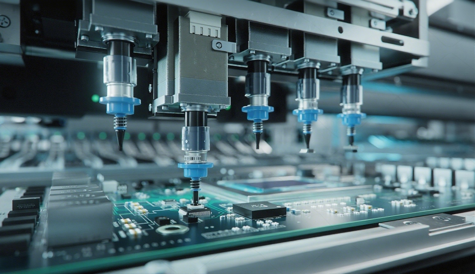
The end mill is the standard tool for milling copper. A two flute cutter clears the chips well in the soft metal, and a carbide tool holds its edge far longer than a high speed steel one.
A V shaped engraving tool is used for isolation routing because its tip can cut a narrow channel with a shallow depth of cut. The width of the cut then depends on how deep the tip is pushed, which couples the spacing to the depth control.
The flute length has to be short enough that the tool does not flex. A long thin tool deflects under the cutting load, and the deflection shows as a trace that is narrower in the middle of a long run than at its ends.
Tool wear changes the effective diameter, so a worn tool cuts a wider channel and reduces the clearance. On a fine pitch board the wear has to be compensated or the tool replaced before the clearance closes.
Spindle Speed and Feed Rate
The spindle speed has to be high enough for the surface speed of the tool to be in the right range for copper. A small tool needs a very high rotational speed to reach that surface speed, which is why a high speed spindle is the defining feature of a milling machine.
The feed rate is the travel speed of the tool through the material. Too high a feed leaves a burr and can snap the tool, and too low a feed rubs the copper and work hardens it. The two parameters are set together, not one at a time.
A conservative starting point is a moderate feed with the highest spindle speed available, then increase the feed until the chips come off cleanly. The sound of the cut is a good guide: a steady note means the load is even, and a chatter means the tool is being pushed too hard.
The copper thickness matters as well, because a one ounce laminate takes twice the cut of a half ounce one. A design that mills well on thin copper may need two passes on the thicker material.
Depth of Cut and Z Axis Control
Depth of cut is the hardest variable to control on a milling machine, because the copper surface is not perfectly flat. The laminate varies in thickness, the bed is not level, and the tool length changes with each change of tool.
The usual solution is a touch off on the surface before cutting, followed by a spring loaded or floating tool holder that keeps a constant pressure. Without one of these, a variation of a few tens of microns across the panel is enough to cut through a trace.
A shallow depth of cut is preferred, so the tool removes only the copper and a thin layer of laminate. Cutting deeper wears the tool faster and widens the channel, which reduces the clearance between traces.
Where the copper is thick, several shallow passes give a better result than one deep pass. The passes also keep the tool cool, which extends its life and reduces the burr on the edge of the copper.
The design should therefore avoid features that demand a deep cut, such as a wide slot in a thick panel. Those features are better routed from the back or formed in a separate operation.
Fixturing, Flatness and Dust
The panel has to be held flat against the bed for the depth control to work. Double sided tape is the common method for a prototype, and a vacuum table is used where the panel size justifies it.
Flatness above all else determines the yield. A panel that bows by a tenth of a millimetre will have some traces cut through and others barely isolated, even though the tool path was correct.
Copper dust is abrasive and conductive, so the machine needs extraction and the board needs cleaning before it is populated. A board that is milled dry and wiped with a dry cloth will leave a film that interferes with soldering.
The board outline is cut with the same machine, often with a larger tool. Keeping the outline and the traces in one setup avoids the registration error that comes from moving the panel, and it makes the tooling holes line up with the copper.
Limits Compared with Etching
Milling cannot reach the resolution of a photolithographic process. Fine pitch components, dense ball grid arrays and narrow traces below a certain width are simply out of reach, and no amount of machine tuning changes that.
The advantage is time and independence. A board can be revised and remilled within an hour, without a phototool or a chemistry line, which is why the process remains popular for prototyping and for a quick second iteration.
The copper surface is also left with a burr and with tool marks, so the solderability is worse than a plated and finished board. A milled board usually needs a light abrasion and a flux that is more active than the one used on a fabricated panel.
The two approaches are therefore complementary: mill for the first article and for a mechanical fit check, then fabricate for the production version. A layout should be designed for the process that will make the production board, not for the prototype.
FAQ
What is the smallest trace width for pcb milling? Around 0.15 to 0.2 mm is a realistic limit with a good machine, and it depends more on the tool life than on the tool diameter.
Can a milled board be used for a final product? It can for a small volume, but the surface finish and the resolution are both worse than a fabricated board. Most teams mill the prototype and fabricate the release.
Why does a milled trace come out narrower in the middle? Tool deflection and a varying depth of cut. A shorter flute length and a constant depth control both reduce the effect.