For hardware developers, electrical engineers, startups, and product teams, one of the most important stages of product development is transforming a digital design into a working physical prototype. A schematic may look perfect in simulation, but only a real PCB can demonstrate how the circuit behaves under actual electrical, mechanical, thermal, and operating conditions.
This is where PCB Prototype Assembly becomes essential.
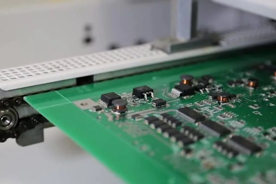
Unlike mass production, Prototype PCB Assembly focuses on rapid manufacturing, engineering validation, flexible component sourcing, and fast design iteration. The purpose is not simply to build a few circuit boards, but to identify design problems early and create a reliable foundation for future production.
With modern manufacturing technologies, integrated PCB fabrication, component sourcing, SMT assembly, testing, and engineering support can significantly shorten the development cycle.
Kingda provides Rapid PCB Prototyping, PCB fabrication, component procurement, SMT/THT assembly, testing, and turnkey PCBA services, supporting prototype quantities without a minimum order requirement. Its published prototype capabilities include SMT and through-hole assembly, fine-pitch component insertion, 01005/0201 components, BGA down to 0.25 mm pitch, AOI and X-ray inspection, and functional testing. (Kingda)
What Is PCB Prototype Assembly?
PCB Prototype Assembly is the process of mounting electronic components onto a fabricated printed circuit board in small quantities for design verification, functional testing, and engineering validation.
Unlike High Volume PCB Assembly, prototype production emphasizes:
- Rapid turnaround
- Low-volume production
- Flexible component sourcing
- Engineering feedback
- Design iteration
- Electrical and functional validation
- Manufacturing risk reduction
A typical prototype PCBA workflow includes:
PCB Design → DFM/DFA Review → PCB Fabrication → Component Sourcing → Solder Paste Printing → SMT/THT Assembly → Reflow/Selective Soldering → AOI/X-Ray → Electrical Testing → Functional Validation
A successful prototype provides engineers with valuable information before the product enters pilot or mass production.
Why Is Prototype PCB Assembly Important?
1. Design Validation
The first physical prototype confirms whether the theoretical circuit actually works as intended.
Engineers can verify:
- Circuit functionality
- Component compatibility
- Power distribution
- Signal integrity
- Thermal behavior
- Mechanical fit
- Connector alignment
- Firmware interaction
This is particularly important for High-Speed PCB, RF, power electronics, IoT, automotive, and medical applications.
2. Faster Engineering Iteration
A prototype allows engineers to find problems before committing to expensive tooling and mass production.
A typical development cycle may be:
Prototype → Test → Identify Problems → Modify Design → Prototype Again
The faster each cycle can be completed, the faster the product can reach production.
3. Firmware and Software Development
For embedded products, software and hardware development often happen simultaneously.
A real prototype provides a platform for:
- Firmware programming
- Driver development
- Communication testing
- Sensor calibration
- Debugging
- Hardware-software integration
4. Lower Production Risk
Discovering a design problem during prototype production is generally much less expensive than discovering the same problem after thousands of units have been manufactured.
Prototype assembly therefore functions as an important risk-control stage in the product-development process.
Challenges of Traditional PCB Prototype Assembly
Traditional prototype manufacturing can create several problems.
High Cost for Small Quantities
Many manufacturers optimize their facilities for larger production volumes. Small orders may therefore have higher setup costs, tooling charges, and engineering costs.
A startup that needs only five or ten boards may not want to commit to a large MOQ.
An effective prototype manufacturer should therefore support Low MOQ PCB Assembly.
Long Lead Times
Prototype production may involve several separate suppliers:
PCB Manufacturer → Component Supplier → Assembly House → Testing Provider
Every additional supplier can create another potential source of delay.
An integrated manufacturer can reduce these handoffs by combining fabrication, sourcing, assembly, and testing.
Component Availability
Prototype BOMs often contain specialized or difficult-to-source parts.
A single unavailable IC can delay the entire prototype.
Professional Component Sourcing for PCB Assembly should therefore include availability checks and alternative-component evaluation.
Quality and Communication Problems
Prototype designs often change quickly.
A reliable manufacturer needs to handle:
- BOM revisions
- Gerber updates
- Component substitutions
- Assembly instructions
- Engineering questions
- Last-minute design changes
Fast communication is therefore just as important as manufacturing speed.
How to Choose a Fast and Cost-Effective Prototype PCB Assembly Service
When evaluating a PCB Prototype Assembly Manufacturer, consider the following factors.
Integrated PCB Manufacturing and Assembly
An integrated supplier can provide:
PCB Fabrication + Component Procurement + PCB Assembly + Testing
This reduces supplier coordination and can shorten the overall production cycle.
Kingda operates as a one-stop PCBA manufacturer integrating PCB manufacturing, component procurement, SMT, DIP/THT, testing, and finished-product assembly. (Kingda)
Low MOQ
Prototype services should accommodate small quantities.
Kingda states that its prototype PCB assembly service has no minimum order quantity requirement. (Kingda)
This makes low-quantity production practical for:
- Startups
- University projects
- R&D teams
- Engineering departments
- New product development
Rapid Turnaround
The manufacturing partner should offer a clearly defined prototype lead time.
Kingda publishes 4–7 day quick-turn rapid PCB prototyping under its prototype service, depending on design and production requirements. (Kingda)
DFM and DFA Support
Design for Manufacturability (DFM) identifies PCB fabrication problems.
Design for Assembly (DFA) evaluates whether components can be assembled efficiently.
Typical checks include:
- Component spacing
- Pad geometry
- Footprints
- Trace width
- Clearance
- Via dimensions
- Solder-mask openings
- Component orientation
Kingda provides DFMA services covering both DFM and DFA. (Kingda)
Prototype PCB Assembly Process
Step 1: Design and Manufacturing File Review
The process begins with the customer’s design files.
Typical documents include:
- Gerber files
- BOM
- Pick-and-place/Centroid file
- Schematic
- Assembly drawing
- PCB stackup
- Special manufacturing requirements
The engineering team reviews the files before production.
Kingda states that its engineering team reviews prototype layouts before manufacturing to identify potential problems and improve cost efficiency. (Kingda)
Step 2: PCB Fabrication
The bare PCB is manufactured according to the design specifications.
Depending on the application, prototype PCBs may include:
- Single-layer boards
- Double-layer boards
- Multilayer PCBs
- HDI PCBs
- Flexible PCBs
- Rigid-flex PCBs
- High-frequency PCBs
- Metal-core PCBs
For prototypes, it is important to use a fabrication process that is compatible with the intended production design.
Step 3: Component Procurement
Once the BOM is reviewed, components are sourced.
A professional procurement process should verify:
- Manufacturer part number
- Availability
- Package
- Quantity
- Lifecycle
- Supplier
- Approved alternatives
Kingda uses an ERP-based component management system and reports a sourcing team of more than 20 purchasing specialists. Its published component-sourcing workflow includes BOM review, quotation, sourcing, and incoming material control. (Kingda)
Step 4: Solder Paste Printing
For SMT assembly, solder paste is deposited onto PCB pads using a stencil.
Accurate solder-paste deposition is critical for small and fine-pitch components.
The process must control:
- Stencil thickness
- Aperture design
- Printing pressure
- Alignment
- Paste volume
Step 5: Component Placement
Automated pick-and-place equipment places components according to the centroid file.
Kingda’s published prototype capabilities include:
- 01005
- 0201
- Fine-pitch components
- BGA
- QFN
- Through-hole components
Its prototype service lists a minimum BGA pitch of 0.25 mm and IC placement precision of approximately ±0.03 mm under the stated capability conditions. (Kingda)
Step 6: Reflow and THT Soldering
After placement, SMT assemblies pass through a controlled reflow process.
For THT components, manufacturers may use:
- Manual soldering
- Wave soldering
- Selective soldering
Kingda supports SMT, through-hole, and mixed assembly, allowing prototype designs with different component technologies to be manufactured through one assembly process. (Kingda)
Step 7: Inspection
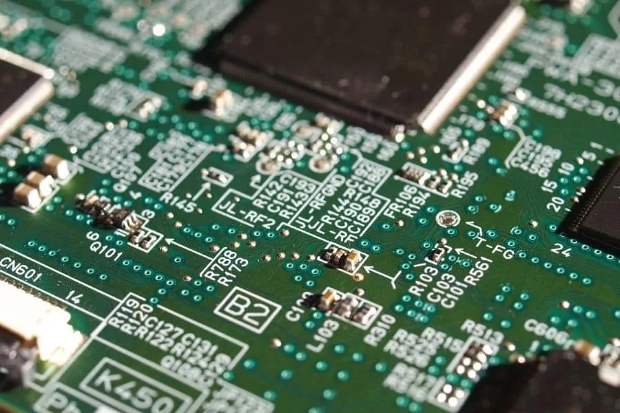
Prototype boards should receive professional inspection even when the quantity is very small.
Common inspection methods include:
AOI
Automated Optical Inspection detects:
- Missing components
- Incorrect placement
- Polarity problems
- Solder defects
X-Ray Inspection
X-Ray Inspection can inspect hidden solder joints, especially for:
- BGA
- QFN
- Bottom-terminated devices
Kingda states that its prototype assembly service includes 100% X-ray and AOI testing. (Kingda)
Step 8: Functional Testing
Functional testing determines whether the finished prototype performs according to the design requirements.
Testing may include:
- Power-up testing
- Communication interfaces
- Sensor functionality
- Motor control
- Display operation
- Wireless communication
- Firmware programming
- Analog measurements
Kingda lists IC programming and functional testing among its prototype PCB assembly capabilities. (Kingda)
Ways to Reduce PCB Prototype Assembly Cost and Lead Time
1. Prepare a Complete BOM
A clean BOM reduces engineering questions and procurement delays.
Include:
- Manufacturer
- MPN
- Description
- Quantity
- Package
- Supplier
- Approved alternatives
2. Use Standard Components
Common, readily available components are generally easier to source than obsolete or highly specialized parts.
This can reduce both sourcing risk and prototype lead time.
3. Prepare Accurate Pick-and-Place Files
The centroid file should include:
- Reference designator
- X coordinate
- Y coordinate
- Rotation
- Component side
Incorrect placement data can delay assembly.
4. Define Alternatives Early
For critical components, engineers can identify approved alternatives before the prototype order is placed.
This prevents the manufacturing process from stopping if the preferred component is unavailable.
5. Optimize Panelization
Small PCB designs can sometimes be panelized to improve assembly efficiency.
Proper PCB Panelization can reduce:
- Machine setup time
- Handling time
- Assembly cost
- Material waste
6. Communicate Special Requirements Early
Special requirements should be communicated before production, including:
- Controlled impedance
- Specific PCB stackup
- Special surface finish
- Conformal coating
- Programming
- Functional testing
- Custom packaging
Kingda PCB Prototype Assembly Advantages
Kingda’s current published prototype services provide several capabilities that are particularly relevant to engineering teams.
No Minimum Order Quantity
Kingda states that its prototype PCB assembly service has no MOQ requirement, allowing customers to produce small quantities for design validation. (Kingda)
Fast Prototype Production
Kingda publishes a 4–7 day quick-turn prototype service, subject to product specifications and production conditions. (Kingda)
Advanced Component Capability
Prototype production supports:
01005 + 0201 + Fine Pitch + BGA + QFN + THT
Kingda lists BGA down to 0.25 mm pitch and IC assembly precision of approximately ±0.03 mm under its published prototype capability. (Kingda)
100% AOI and X-Ray
Kingda’s rapid prototype service lists 100% AOI and X-ray testing, providing additional quality assurance for prototype assemblies. (Kingda)
Component Procurement
Kingda provides integrated PCB Component Procurement, supported by ERP-based inventory management and a sourcing team of more than 20 purchasing specialists. (Kingda)
One-Stop Manufacturing
Kingda can integrate:
PCB Design → PCB Fabrication → Component Procurement → SMT/THT → Testing → Box Build
This makes it possible to keep prototype manufacturing and later production under one manufacturing partner. (Kingda)
Quality Management
Kingda reports ISO 9001, ISO 13485, and IATF 16949 quality-management certifications and provides manufacturing services for medical, automotive, industrial automation, AI, smart-home, security, power, and communications applications. (Kingda)
Prototype PCB Assembly vs. Mass Production
| Feature | PCB Prototype Assembly | Mass PCB Assembly |
|---|---|---|
| Quantity | 1–hundreds | Thousands+ |
| Main objective | Design validation | Production efficiency |
| Lead time | Short | Planned/optimized |
| Engineering changes | Frequent | Controlled |
| Component sourcing | Flexible | Long-term supply planning |
| Testing | Design verification | Automated production testing |
| Cost priority | Development cost | Unit cost |
| Production flexibility | Very high | Highly standardized |
| Best application | R&D and new products | Established products |
A good manufacturing partner should ideally support both stages, allowing the product to transition from prototype to production without unnecessarily changing suppliers.
When Should You Use Prototype PCB Assembly?
PCB Prototype Assembly is particularly useful when:
- Developing a new electronic product
- Validating a new PCB design
- Testing high-speed circuits
- Testing power electronics
- Developing IoT devices
- Integrating firmware and hardware
- Evaluating thermal performance
- Preparing for regulatory testing
- Preparing for pilot production
- Testing mechanical integration
For complex products, multiple prototype iterations may be necessary before the design is ready for mass production.
Conclusion
PCB Prototype Assembly is a critical bridge between electronic design and successful mass production.
A high-quality prototype allows engineers to verify electrical performance, validate mechanical integration, develop firmware, identify manufacturing problems, and refine the design before large-scale production begins.
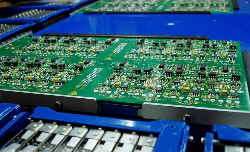
The most effective prototype manufacturing strategy combines:
Fast PCB Fabrication + Reliable Component Sourcing + DFM/DFA + Precision SMT/THT Assembly + AOI/X-Ray + Functional Testing
Kingda provides an integrated Rapid PCB Prototyping and Prototype PCB Assembly service with no MOQ, 4–7 day rapid prototype capability, advanced SMT packages, component procurement, AOI/X-ray inspection, IC programming, functional testing, and a production path from prototypes to volume manufacturing. (Kingda)
For startups, engineering teams, OEMs, and product developers, choosing an experienced PCB Prototype Assembly Manufacturer can significantly reduce development risk, shorten iteration cycles, and create a smoother transition from prototype to production.