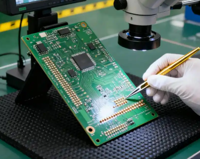
PCB Prototype production is typically carried out in small quantities to verify circuit performance, mechanical fit, and manufacturing feasibility. At this stage, manufacturers can often accommodate designs that are not fully optimized for automated, high-volume production. However, a design that works well for prototypes may encounter significant problems when transferred to mass production.
Without considering production requirements early in the development process, companies may experience lower yields, assembly defects, dimensional problems, or even require a new PCB revision before volume production can begin. Therefore, designing for a smooth transition from PCB Prototype production to Mass Production is an important part of new product development.
This consideration is especially important for applications such as medical monitoring equipment, industrial control modules, automotive electronics, communication systems, and other products that require consistent production quality. Early attention to manufacturing compatibility can reduce redesign risks, improve production stability, and lower the total cost of manufacturing.
Why Prototype Designs May Fail in Mass Production
The manufacturing conditions for prototypes and Mass Production are not identical. Prototype production may rely more heavily on manual operations, flexible equipment settings, and engineering intervention. By contrast, volume production depends on standardized processes, automated equipment, optimized panel utilization, and tightly controlled process windows.
A prototype PCB may therefore pass functional testing while still having hidden manufacturing risks.
Common transition problems include:
- Insufficient panelization features for automated assembly
- Inadequate fiducials or tooling holes
- Component spacing that is too tight for production tolerances
- Difficult soldering conditions for fine-pitch components
- Trace and spacing dimensions with insufficient process margin
- Hole, board-edge, or mechanical dimensions without adequate tolerance
- Uneven copper distribution that affects lamination and etching
- PCB dimensions that are difficult for automated handling equipment
- Assembly defects caused by thermal imbalance
- Increased scrap rates during volume manufacturing
These problems are often not caused by a fundamental circuit design error. Instead, they result from insufficient consideration of DFM requirements during the prototype stage.
Four Major Areas of Prototype-to-Production Compatibility
1. Panelization and Automated Manufacturing
One of the most common differences between prototype and production manufacturing is panelization.
Prototype boards are often manufactured as individual pieces because the production quantity is small. In volume production, however, multiple PCBs are commonly arranged into a production panel to improve equipment efficiency and reduce handling time.
A production-ready panelization strategy should consider:
- PCB dimensions and board shape
- Panel utilization
- Tooling holes
- Fiducial marks
- Board orientation
- Assembly direction
- V-groove or routed separation
- Component-to-edge clearance
- Depanelization requirements
- Automated conveyor and fixture requirements
For example, a PCB without suitable fiducial marks may be difficult for automated placement equipment to accurately recognize. Insufficient tooling features can also affect board positioning during assembly and inspection.
Instead of creating the panel only after the prototype has been approved, the panelization concept should be considered during the PCB Design stage. The prototype can then be manufactured using a representative production panel when practical, allowing potential automation problems to be identified earlier.
2. Component Layout and Assembly Compatibility
Component placement is another major factor affecting the transition from prototype production to PCB Assembly at scale.
During prototype assembly, engineers may be able to manually correct minor placement or soldering problems. Automated production requires considerably more consistent component spacing, orientation, thermal conditions, and soldering conditions.
The layout should therefore consider:
- Minimum spacing between components
- Component-to-board-edge clearance
- Fine-pitch IC placement
- BGA and QFN assembly requirements
- Tall-component interference
- Connector accessibility
- Heat-generating components
- Thermal distribution
- Rework accessibility
- Automated inspection requirements
Fine-pitch devices require particular attention. The pad geometry, solder-mask design, stencil apertures, and component spacing should be reviewed together rather than independently.
For BGA, QFN, and other components with hidden solder joints, the design should also allow an appropriate inspection strategy, such as X-ray inspection where required.
High-power components should be positioned with thermal distribution in mind. Concentrating several heat-generating components in one area may create local temperature differences during reflow, potentially increasing the risk of soldering defects or component stress.
3. Manufacturing Tolerance and Process Margin
A prototype can sometimes be manufactured successfully even when its design is close to the limits of the manufacturing process. This does not necessarily mean that the same design will remain stable during volume production.
Manufacturing Tolerance should therefore be considered from the beginning.
Important dimensions include:
- Trace width and spacing
- Minimum hole diameter
- Annular ring
- Hole-to-copper clearance
- Board thickness
- Dielectric thickness
- Board outline
- Slot dimensions
- Component placement tolerance
- Board-edge clearance
- Registration between layers
For multilayer PCBs, additional attention should be given to inner-layer registration, lamination, drilling, copper distribution, and finished dielectric thickness.
A design that uses extremely narrow traces or very small clearances may leave little process margin. During volume production, normal variations in imaging, etching, drilling, lamination, and registration can then have a greater effect on yield.
The goal is not simply to make the PCB as compact as possible. The design should provide an appropriate balance between electrical performance, mechanical requirements, density, and manufacturing capability.
4. Mechanical and Structural Compatibility
Mechanical compatibility is equally important when moving from prototype to production.
A prototype may fit correctly during manual assembly, but small dimensional deviations can become more significant when thousands of boards are produced and assembled into an enclosure.
The design should therefore define suitable tolerances for:
- Overall PCB dimensions
- Mounting holes
- Hole locations
- Slots and cutouts
- Board-edge features
- Connector positions
- Keep-out areas
- Component height
- Edge clearance
Board edges should also be compatible with the selected fabrication and depanelization process. Designs with extremely narrow edge structures or complex cutouts may require additional manufacturing review.
For products with tight mechanical interfaces, the PCB should be evaluated together with the enclosure, connectors, cables, heat sinks, brackets, and other mechanical components.
How to Design a PCB for a Smooth Prototype-to-Production Transition
Plan Panelization During the Prototype Stage
Panelization should not be treated as a final manufacturing activity.
During the prototype phase, engineers can develop a preliminary production panel that includes appropriate tooling holes, fiducials, rails, and separation features. This approach allows the assembly process to be evaluated under conditions that more closely represent volume production.
The panel design should also consider component orientation and automated equipment requirements.
Where practical, the prototype and production versions should use the same basic panelization concept. This reduces the risk of discovering assembly problems only after production quantities have increased.
Optimize Component Spacing
Component placement should provide sufficient clearance for automated assembly, soldering, inspection, and rework.
Particularly sensitive areas include:
- Fine-pitch ICs
- BGA packages
- QFN packages
- Small passive components
- Connectors
- Large electrolytic capacitors
- Transformers
- Heat sinks
- High-power devices
Component spacing should be reviewed together with the expected placement accuracy, stencil design, soldering process, and inspection method.
Design Adequate Process Margins
A production-oriented PCB Design should avoid unnecessarily pushing manufacturing dimensions to their absolute limits.
For example, if a trace width is reduced to achieve higher routing density, engineers should also evaluate its impact on etching capability, impedance, current capacity, and production yield.
Similarly, very small holes may increase drilling and plating complexity. A reasonable design margin can make the board more tolerant of normal manufacturing variation.
The appropriate margin depends on the PCB structure, materials, fabrication technology, and manufacturer’s actual process capability. Therefore, designers should confirm critical limits with the PCB manufacturer before releasing the design.
Balance Copper Distribution
Copper distribution is particularly important for multilayer boards.
Large differences in copper density between different areas of a panel can affect etching, lamination, resin flow, thermal behavior, and finished dielectric thickness.
For high-density and impedance-controlled boards, engineers should review:
- Inner-layer copper distribution
- Reference-plane continuity
- Large isolated copper areas
- Copper imbalance between layers
- Thermal relief structures
- High-current copper areas
- Power and ground plane distribution
Balanced copper distribution can help improve manufacturing consistency and reduce process-related variation.
Consider DFM Before Prototype Fabrication
DFM is one of the most effective ways to reduce prototype-to-production problems.
A comprehensive DFM review can evaluate:
- Stackup and material selection
- Minimum trace and spacing requirements
- Hole sizes and aspect ratios
- Annular rings
- Copper thickness
- Solder-mask clearance
- Silkscreen placement
- Panelization
- Tooling and fiducials
- Component-to-edge clearance
- Assembly accessibility
- Testing requirements
The purpose of DFM is not to restrict the PCB designer. Instead, it helps identify potential manufacturing risks while changes are still inexpensive and easy to implement.
Simulating the Mass-Production Process During Prototype Runs
A useful strategy is to use the prototype stage as an early production-readiness validation step.
Instead of checking only whether the circuit works, engineers can evaluate the complete manufacturing flow:
PCB fabrication → panelization → SMT placement → reflow soldering → THT assembly → inspection → electrical testing → depanelization → final assembly
This approach can reveal problems that electrical testing alone cannot detect.
For example, the prototype may function correctly but still have:
- Difficult board handling
- Poor fiducial recognition
- Stencil printing limitations
- Component clearance problems
- Reflow thermal imbalance
- AOI inspection limitations
- Difficult depanelization
- Mechanical assembly interference
Identifying these issues during prototype production is generally easier than correcting them after production volumes increase.
Prototype and Mass Production Design Comparison
| Design Factor | Prototype-Oriented Design | Production-Oriented Design |
|---|---|---|
| Production quantity | Small | Medium to high |
| Panelization | May be optional | Usually planned |
| Tooling holes | May be limited | Typically required for automated processes |
| Fiducials | May be minimal | Important for automated assembly |
| Component spacing | Can be relatively compact | Must consider process capability |
| Manufacturing tolerance | May have limited consideration | Must be defined and controlled |
| Automation | Limited or flexible | Highly standardized |
| Inspection | Engineering-focused | Automated and standardized |
| Process margin | May be relatively narrow | Requires appropriate margin |
| Cost optimization | Development priority | Yield and throughput become important |
The objective is not to make prototype production identical to high-volume production in every detail. Instead, the prototype should validate the design under conditions that expose the most important production risks.
Common Prototype-to-Production Problems and Solutions
| Problem | Possible Cause | Recommended Approach |
|---|---|---|
| Placement offset | Insufficient fiducials or board positioning features | Add suitable fiducials and tooling features |
| Solder bridging | Tight pitch or unsuitable stencil aperture | Review pad and stencil design |
| Tombstoning | Uneven thermal or solder conditions | Improve component layout and thermal balance |
| Poor AOI coverage | Component arrangement or inspection limitations | Review component orientation and inspection access |
| Board dimension variation | Insufficient mechanical tolerance | Define appropriate fabrication tolerances |
| Open or short circuits | Excessively tight trace/space design | Review manufacturing capability and process margin |
| Difficult depanelization | Poor panel or routing design | Optimize V-groove/routing strategy |
| Lamination variation | Uneven copper distribution or stackup sensitivity | Review copper balance and lamination design |
| Assembly interference | Insufficient component clearance | Check enclosure and component height constraints |
The Role of Kingda in Prototype-to-Production Manufacturing
Kingda can support the transition from prototype development to production by integrating manufacturing considerations into the PCB development process.
A production-oriented workflow can include DFM review, PCB fabrication, panelization planning, SMT and THT PCB Assembly, inspection, and production validation.
By reviewing manufacturability before volume production, potential issues involving board dimensions, component placement, panelization, routing, holes, and manufacturing tolerances can be identified earlier.
For products moving from prototype quantities to larger production volumes, maintaining consistent design data and revision control is also important. Changes made after prototype validation should be documented and reviewed before production release to avoid manufacturing discrepancies.
Best Practices for Prototype-to-Mass-Production Compatibility
To improve production readiness, PCB designers should consider the following practices:
- Plan PCB Design requirements with the final manufacturing process in mind.
- Review panelization before prototype fabrication.
- Include appropriate tooling holes and fiducial marks.
- Maintain sufficient component spacing.
- Avoid unnecessary use of extreme manufacturing dimensions.
- Define critical Manufacturing Tolerance requirements.
- Balance copper distribution across multilayer boards.
- Review thermal distribution around high-power components.
- Consider automated assembly and inspection requirements.
- Perform DFM before releasing the prototype.
- Use prototype production to validate the intended manufacturing process.
- Maintain controlled PCB, BOM, Gerber, drill, stencil, and assembly data.
- Complete a formal engineering review before transitioning to Mass Production.
Conclusion
A successful PCB Prototype does not automatically guarantee successful Mass Production. Prototype manufacturing and volume production operate under different equipment, automation, tolerance, panelization, and process-control conditions.
By considering Panelization, component placement, Manufacturing Tolerance, copper distribution, mechanical interfaces, automated assembly, and DFM requirements during the early design stage, engineers can reduce the risk of production-related redesigns.
The most effective approach is to treat prototype production as an opportunity to validate not only electrical performance, but also manufacturing compatibility. With early production planning and systematic DFM review, the transition from prototype to Mass Production can become more predictable, reducing avoidable yield losses, engineering changes, and manufacturing costs.
Kingda can support PCB development and manufacturing workflows with a production-oriented approach, helping engineers evaluate manufacturability and prepare PCB designs for a smoother transition from prototype validation to volume production.