PCB Prototyping to Full Product Design: The Complete Flow
Most descriptions of the design process treat it as one long sequence. In practice it splits into two stages with different goals, different people and different tools. PCB prototyping is exploratory work done by the engineer who understands the application. Product development is production work done by specialists who understand manufacturing.
Confusing the two stages is expensive. A prototype optimized for manufacturability wastes time early; a production design that still carries prototype shortcuts fails later. Knowing which stage the project is in decides what to optimize and which tool to open.
Why Prototyping Exists as a Separate Stage
A prototype answers a question the specification cannot answer on its own: does this approach actually work? It gives an engineer a way to test an idea before committing to a layout that costs money and weeks to change. The goal is not a perfect board but a board that produces useful information.
Failures found during PCB prototyping are cheap. A wrong op-amp configuration, a filter that oscillates or a converter that will not start costs a few days at this stage and a great deal more after tooling, certification and production orders are in motion.
<img src="https://www.gopcba.com/wp-content/uploads/2026/05/彩色多普勒超声驱动PCBA-2.png" alt="PCB prototyping flow from schematic capture to layout” />
Step One: Component Selection and Research
Component selection starts from the requirements and works backward to parts. Supply voltage, signal bandwidth, noise floor, load current and environmental range narrow the field quickly. For each critical part, the designer checks the datasheet conditions rather than the headline specification.
Availability matters as much as performance. A part with a twelve-week lead time or a single supplier can stop a program even when it is electrically ideal. Where an alternative exists, the reference design should tolerate a second source without a layout change.
Step Two: Schematic Capture
Schematic capture turns the chosen parts into a netlist. The work is less about drawing than about discipline: connecting power and ground correctly, assigning designators consistently, and attaching footprint names that match what the fabricator will place.
Good schematics are readable by someone who did not draw them. Signals flow in one direction, decoupling is shown next to the device it serves, and notes record design intent such as why a resistor value was chosen or which interfaces are isolated.
Simulation Before Layout
Simulation answers questions that would otherwise require a board. Transient analysis checks startup and load steps, AC analysis confirms loop stability and filter response, and signal integrity checks estimate whether a fast interface will close its timing budget.
Simulation is not a substitute for measurement, but it moves the discovery of fundamental problems to the cheapest possible moment. A converter with an unstable loop should fail in the simulator, not on the bench after the layout is finished.
Step Three: Board Layout
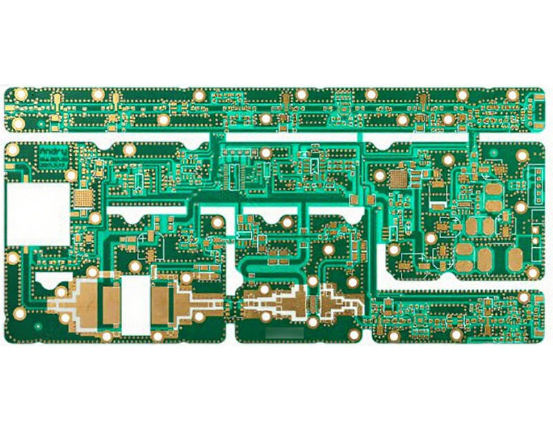
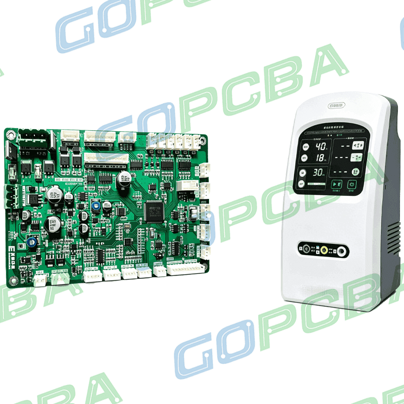
Layout converts the netlist into copper. Placement comes first: connectors at the edges, power components grouped around the converter, sensitive analog blocks isolated from switching nodes, and thermal paths short. Routing follows, with controlled impedance lines treated as constraints rather than suggestions.
Prototype layouts accept some risk in exchange for speed. Production layouts do the opposite. Plane integrity, current density, creepage distances, silkscreen reference designators and test point access are all resolved before the design is released for fabrication.
Step Four: Verification
Design verification happens twice: once on the screen and once on the bench. On screen, the layout is checked against the schematic, clearances are audited, and the stencil and assembly drawings are cross-checked against the bill of materials.
On the bench, the assembled board is powered in a controlled sequence. Current draw is checked before the supply is applied to sensitive rails, rails are sequenced, and each functional block is validated individually before the whole system is exercised.
Where Product Development Takes Over
Product development assumes the function works and asks whether it can be built repeatedly. Design for manufacturability review, panelization, tooling decisions and tolerance stack-up dominate. Yield data from the line replaces bench intuition as the measure of quality.
This is also where documentation becomes a deliverable. Fabrication notes, assembly notes, test procedures and revision control are part of the design, not paperwork added afterward. A design that cannot be reproduced is not finished.
Common Prototyping Mistakes
Three mistakes account for most extra iterations. The first is leaving test points off the board and trying to probe fine-pitch pads with a scope probe. The second is ignoring the power architecture: a rail that cannot supply the transient current the load demands will show up as resets long after the digital design is proven.
The third is a ground strategy chosen by accident. Prototype boards often use whatever plane is left over after routing, and the resulting return paths differ from board to board. Decide the ground arrangement before placing parts, and record it in the schematic so the production layout inherits the decision rather than rediscovering it.
Choosing Tools for Each Stage
Prototyping favors tools with fast schematic entry, easy simulation and a short path from schematic to layout. Product development favors rule-driven layout, library control and output generation for fabrication and assembly.
Most teams use the same suite for both and accept the compromise. The important decision is which features to enforce. Enforce design rules in product development; keep them advisory during prototyping, where exploration matters more than repeatability.
Keeping Prototype Iterations Low
The measure of a prototyping stage is how few iterations it takes to reach a design that meets specification. That number drops when critical assumptions are simulated first, when the layout respects the parts that carry the risk, and when test points are designed in rather than added later.
Once the specification is met, the board should be frozen and handed to product development. Continuing to explore after that point reopens decisions that the production layout depends on, and the cost of each change grows with every step toward the factory.
The wider sequence, from bare board through assembly and test, is covered in PCBA development process. Characteristics that separate a good design from a merely working one are described under PCB design quality characteristics, and the basics of the board itself are explained in PCB circuit board explained.
Documentation That Survives the Handoff
Prototype work still needs records, even when it happens fast. Keep the schematic, the bill of materials and the layout revision aligned, and note every modification made on the bench. A prototype that works but cannot be explained forces the production team to repeat experiments that were already completed.
Revise the documentation at the moment a change is proven, not at the end of the project. The changes made during debugging are exactly the ones that carry the design intent, and they are the first things forgotten once the board finally works.
FAQ
How many prototype iterations should a design need? One or two is normal for a well-understood circuit, and three is a sign that the requirements were not fixed before layout started. If a fifth iteration is required, the problem is usually in the specification rather than the board.
Can simulation replace the first prototype entirely? No. Simulation has no model for solder defects, cable resonance, mechanical tolerances or the layout parasitics that appear at the board edges. It reduces the number of iterations rather than removing the first build.
Who should own the layout in each stage? The prototyping engineer owns it until the function is proven, because rapid change matters more than rule compliance. Product development should then be handed to a layout specialist who works against manufacturing constraints.