Right-Angle Routing in PCB Layout: Impedance and Reflection
Avoiding right-angle routing is one of the first rules a new board designer learns, and it is repeated so often that it is rarely examined. The rule is not superstition, but it is also not the catastrophe that some guidelines imply. Understanding what a corner actually does to a transmission line explains both why the rule exists and when it can safely be relaxed.
How Right Angles Became a Design Rule
The origin is a genuine physical effect. At a right angle the effective width of the trace changes at the corner, and a change in width means a change in characteristic impedance. Obtuse and acute angles produce the same problem to different degrees, so the issue is really about geometry in general rather than about ninety degrees specifically.
Three consequences follow. The corner behaves as a capacitive load that slows the rise time of the signal. The impedance discontinuity reflects part of the incident energy back toward the source. And the sharp point of an acute corner concentrates current, which radiates. None of these effects is large on a low speed signal, which is why the rule is often applied more strictly than the physics requires.
The Corner as a Capacitive Load
The parasitic capacitance of a corner can be estimated from an empirical relationship in which the capacitance in picofarads equals sixty one times the trace width in inches, multiplied by the square root of the relative permittivity, divided by the characteristic impedance. Feeding realistic numbers into that expression shows the effect is small: a corner adds a fraction of a picofarad rather than a meaningful lumped load.
Small does not mean irrelevant. A capacitive discontinuity slows the edge slightly and, more importantly, it is the mechanism that creates the mismatch described below. The capacitance also grows with trace width, so wide power or low impedance traces produce a larger corner effect than a narrow signal trace does.
Impedance Discontinuity and Reflection
Because the effective width increases at the corner, the local impedance falls below the nominal value of the transmission line. The reflection coefficient is then given by the difference between the local impedance and the line impedance divided by their sum, the standard expression for a mismatch between two impedances.
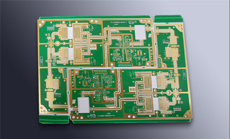
Measured values put the impedance change caused by a right angle in the range of seven to twenty percent, which corresponds to a reflection coefficient of about 0.1 at worst. In decibels that is roughly twenty decibels of return loss, a figure that most digital interfaces tolerate comfortably. The discontinuity is real, but it is modest, and it is only one of many reflections present in a typical channel.
When the Effect Actually Matters
What decides whether the corner matters is the relationship between the signal rise time and the electrical size of the discontinuity. A corner is physically tiny, on the order of the trace width, so its electrical length is a small fraction of a wavelength at ordinary frequencies. When the rise time is much longer than the time it takes a wave to traverse the corner, the discontinuity is averaged out and the signal never sees it.
The situation changes as edges become faster. When the rise time falls to tens of picoseconds, the same corner represents a significant fraction of the transition, and the reflection begins to distort the eye diagram. Radio frequency and microwave designs are affected differently again, because there the corner acts as a small radiator. The relevant transmission line behaviour is covered in microstrip and stripline routing.
Acute and Obtuse Angles, Stubs and Tees
If impedance change were the only concern, a forty five degree corner would be preferable to a right angle, and an arc better still, because both reduce the width perturbation at the bend. That is the practical reason for chamfering: it makes the transition gradual rather than abrupt.
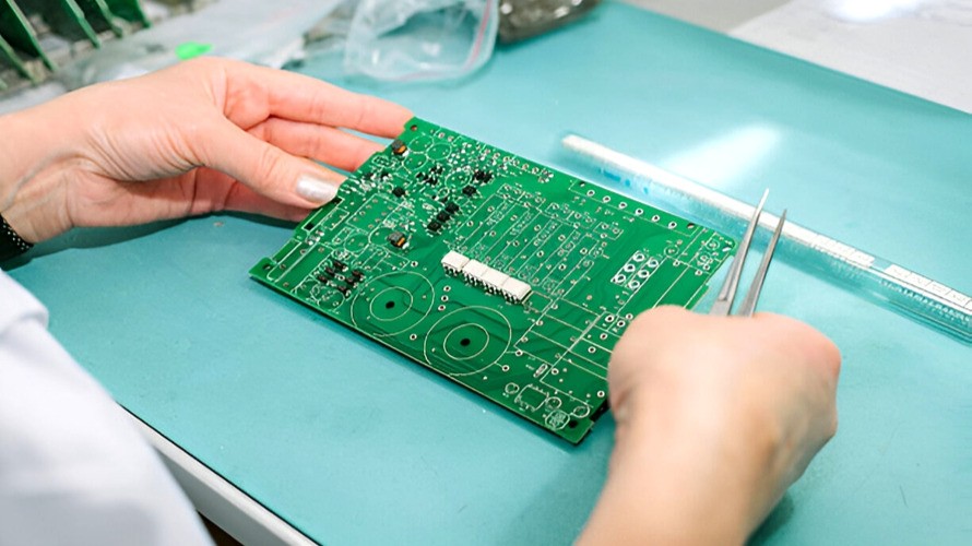
There is a manufacturing argument as well. Sharp inner corners can trap etchant during processing, which over-etches the copper and shifts the impedance further from target. That effect belongs to fabrication rather than to signal integrity, but the remedy is the same. Far more damaging than any corner, however, are stubs, tees and abrupt reference plane changes, all of which produce discontinuities orders of magnitude larger. Fixing those before worrying about corners is the correct order of priority; differential pairs and their specific requirements are discussed in right angle routing in differential traces.
Practical Routing Practice
Chamfer corners at forty five degrees or use a short arc, with a chamfer length of about one and a half to two times the trace width as a working starting point. Keep the reference plane continuous beneath the bend so that the return current does not have to detour, and avoid changing layers at a corner, since a via introduces a far larger discontinuity than the corner ever would.
For critical nets, the useful disciplines are to keep discontinuities short relative to the rise time, to avoid unnecessary layer transitions, and to verify the result rather than assume it. Three dimensional field simulation for the critical channel, or a time domain reflectometry measurement on a test coupon, answers the question directly. Where long traces carry fast data across a board, the guidance in high frequency traces and data bus routing is more relevant than the corner rule itself.
Design Rules That Survive Review
The sensible position is that corners matter at the margin. Chamfering costs nothing, so there is no reason to leave a right angle on a high speed net. But a design should not be delayed over corner geometry while stubs, plane splits and unmatched via transitions remain unaddressed, because those dominate the measured result.
Equally, a low speed board with modest edge rates does not need arcs on every trace. Rule of thumb guidance has value when it encodes physics, and loses value when it is applied without reference to rise time, frequency or the electrical size of the feature being discussed.
Corners in Impedance-Controlled Designs
On an impedance-controlled board the corner question becomes part of a larger tolerance budget. Fabrication already introduces variation in trace width, dielectric thickness and copper roughness, and the resulting impedance spread is typically plus or minus ten percent. A corner whose effect sits inside that band is not the limiting factor, and chasing it while ignoring the wider tolerance is a misallocation of effort.
What does deserve attention is consistency. Every corner in a matched group should use the same geometry, so that the two halves of a differential pair experience the same perturbation and the skew between them stays controlled. Reference plane continuity through the bend matters for the same reason, since an interrupted return path changes the effective impedance far more than the corner itself. It is also worth confirming the geometry with the fabricator, because the artwork decision, the etch compensation and the actual measured impedance are three different things, and only the last one describes the delivered board.
FAQ
Do right angles really ruin signal integrity? They change the trace impedance by roughly seven to twenty percent, producing a reflection coefficient near 0.1. That is a modest discontinuity and is usually acceptable unless the edge rate is extremely fast.
Why chamfer corners at forty five degrees? Chamfering spreads the width change over a short transition instead of an abrupt one, which reduces the impedance mismatch and avoids the sharp inner corners that can trap etchant during fabrication.
What is more important than corner geometry? Keeping the reference plane continuous, avoiding stubs and tees, and limiting layer transitions. Those discontinuities are far larger than anything a corner introduces.