Trace Width and Current Capacity in PCB Design
A trace is a resistor, a heat sink and a fuse at the same time, and the current it can carry depends on how much heat it can lose. That is why the same trace width is safe on an outer layer and marginal on an inner layer, and why a width copied from a table is only a starting point.
The calculation is not difficult, but it depends on assumptions that are easy to leave unstated: the permitted temperature rise, the copper weight, the ambient temperature and the presence of copper nearby that can help carry heat away.
The Temperature Rise Question
The usual basis for a width calculation is an allowed temperature rise above ambient, commonly ten degrees Celsius for a conservative design. The figure is a choice rather than a rule, because a rise that is acceptable in a ventilated enclosure may be unacceptable inside a sealed one.
A higher permitted rise allows a narrower trace, and a lower one requires a wider trace or a heavier copper weight. The choice should be made with the enclosure and the neighbouring components in mind rather than from habit.
Copper Weight and Thickness
A one ounce copper layer is about thirty five micrometres thick, and doubling the weight doubles the cross section for the same width. Heavier copper is therefore the direct route to more current capacity without using more board area.
The trade is etch capability, since a heavy layer cannot hold the same fine features as a light one. A design that needs heavy copper for a power path and fine pitch for a controller usually separates the two onto different layers.
Outer Layer Against Inner Layer
An outer trace loses heat to the air and to the laminate, while an inner trace loses heat only to the laminate, which is a much poorer conductor. The same geometry therefore runs hotter inside the board, and the derating is typically a factor of about two in current for the same width.
This is why power routing is preferred on the outer layers where the geometry allows it. Where an inner layer is unavoidable, the width should be increased or the copper weight raised to compensate.
Fusing Current and Short Duration Loads
The fusing current is the level at which the trace melts, and it is far above the steady state rating because the trace has thermal mass. A trace that carries a short pulse can therefore be much narrower than one that carries a continuous current.
Care is needed with this reasoning, because the trace is not a fuse and its behaviour at the fusing level is neither repeatable nor safe. Pulse ratings are useful for an inrush condition, not as a design target.
Vias and Layer Changes
A via has less copper cross section than the trace it connects, so a layer change is a local hot spot unless several vias are used or the via is filled. The resistance of a single small via can exceed that of a long trace on a heavy layer.
The usual remedy is a cluster of vias at each transition, with the count chosen from the current rather than from the space that happens to be available. The same reasoning applies to thermal paths where the vias carry heat instead of current.
Ambient and Neighbouring Heat Sources
The rise is measured above the local ambient, not above the room temperature. A trace that runs beside a regulator or under a power inductor starts from a higher baseline, so its permitted rise is consumed before any current is applied.
Where the environment is hot, the derating should be applied to the base figure and not to the rise. A design that is marginal at twenty five degrees is not fixed by a wider trace alone if the local air is already at eighty.
Copper Area, Planes and Heat Spreading
A trace connected to a plane sheds heat into that plane, which raises its capacity above the isolated value. This is why a short trace between a plane and a component often carries more current than a table predicts.
The effect works in the other direction as well, since a trace that is isolated on a narrow neck cannot use the plane around it. The width should be judged over the narrowest section of the path rather than at the widest.
Voltage Drop and Impedance
Current capacity is only one criterion, and the resistance of the path may set the width first. A supply trace that drops a tenth of a volt over its length may be within its thermal rating and still fail the device specification.
The calculation is the resistivity of copper, the length and the cross section, and it should be done for the worst case temperature since resistance rises with heat. Where a sense line or a reference is involved, the drop matters even at low current.
Layout Practice
Where a design is tight, the current path should be routed first and everything else arranged around it. Widening a trace after the layout is complete is rarely possible without moving components, so the decision belongs early.
It also helps to keep the return path beside the supply path, both for the loop area and for the heat, since the two conductors share the thermal load. This is the same principle that the general rules for design guidelines apply to other constraints.
Verification
The finished design should be checked against the calculation, either by an automated rule with the right assumptions or by a manual review of the narrow sections. A temperature measurement on a prototype is the confirmation that the assumptions were reasonable.
Where a board runs warm, an infrared image shows which trace is hot, and the answer is often a bottleneck that no single section of the drawing made obvious. Measuring is faster than arguing about a table.
Process Control and Verification
On a design of this kind, current capacity is the item that decides how the rest of the board is arranged. The process window is set by the narrowest step in the flow, so an improvement anywhere else shows up as margin rather than as yield until that step is addressed. A short note on the drawing about handling, storage or packaging is often worth more than an extra decimal place on a tolerance.
Related reading: our fabrication notes, board quality and design release notes cover the same ground.
Process Control and Verification
On a design of this kind, current capacity is the item that decides how the rest of the board is arranged. The process window is set by the narrowest step in the flow, so an improvement anywhere else shows up as margin rather than as yield until that step is addressed. A short note on the drawing about handling, storage or packaging is often worth more than an extra decimal place on a tolerance.
A first article check confirms that the process and the drawing agree on the points listed above, and that the coupon data supports the values used in the design.
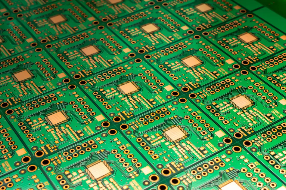
Where a measurement falls outside the expected window, the sample is retained so that the cause can be established before the balance of the batch is released.
A first article check confirms that the process and the drawing agree on the points listed above, and that the coupon data supports the values used in the design.
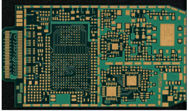
Where a measurement falls outside the expected window, the sample is retained so that the cause can be established before the balance of the batch is released.
FAQ
Is there a single table for trace width? No. The tables assume a temperature rise, a copper weight and an environment, and the assumptions should be stated with any figure that is used.
How much does an inner layer derate? Commonly by about half the current for the same width, depending on the stack up and the surrounding copper.
Can a fuse be replaced by a narrow trace? It should not be. A trace is not repeatable at its fusing level, and a protective device belongs in the circuit.
What is the most common mistake? Judging the width at the widest point of the path instead of at the neck where the current actually concentrates.