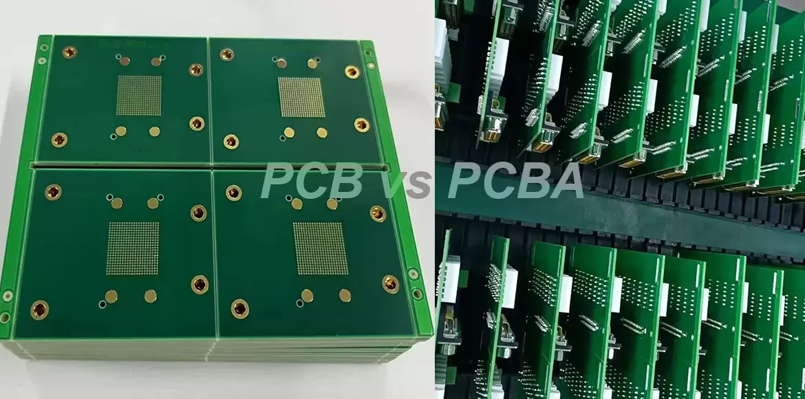
In electronics manufacturing, PCB vs PCBA is a common topic because both are essential to the development and production of electronic products.
A PCB (Printed Circuit Board) provides the physical and electrical foundation of an electronic system. A PCBA (Printed Circuit Board Assembly) is a completed assembly in which electronic components are mounted and soldered onto the PCB.
Although PCB and PCBA are closely related, they involve different technologies, processes, and quality requirements. Rather than simply asking which one has a higher technical level, it is more accurate to understand how their technical challenges differ across design, manufacturing, assembly, and testing.
PCB Design vs PCBA Design
PCB Design
PCB Design is the foundation of an electronic product. It transforms a circuit schematic into a physical circuit structure that can be manufactured and assembled.
A professional PCB design may involve:
- Circuit architecture
- Component placement
- PCB layout
- Signal routing
- Power distribution
- Grounding
- Impedance control
- Signal integrity
- Thermal management
- Electromagnetic compatibility
- Manufacturability
- Reliability
For high-speed and high-density products, PCB Design can become highly complex.
Engineers must carefully control trace width, spacing, layer stackup, via structures, return-current paths, power integrity, and impedance.
For example, high-speed interfaces such as PCIe, USB, Ethernet, DDR, and other high-frequency signal paths may require strict control of routing geometry and dielectric characteristics.
Therefore, advanced PCB design requires not only knowledge of circuit theory but also an understanding of materials, manufacturing capabilities, signal integrity, and system requirements.
PCBA Design
PCBA Design is closely connected to PCB design but focuses more heavily on component integration and assembly considerations.
The designer must consider:
- Component selection
- Component package types
- Component placement
- Solderability
- Assembly process
- Thermal distribution
- Signal integrity
- Mechanical clearance
- Inspection accessibility
- Rework requirements
A PCB may be electrically correct but still difficult to assemble if the component placement, pad design, thermal design, or manufacturing tolerances are not properly considered.
Therefore, good PCBA Design requires close coordination between electrical design and assembly engineering.
PCB Manufacturing vs PCBA Manufacturing
PCB Manufacturing
PCB Manufacturing converts the PCB design data into a physical circuit board.
Depending on the board type, the process may include:
- Material preparation
- Inner-layer imaging
- Etching
- Lamination
- Drilling
- Copper plating
- Outer-layer imaging
- Solder mask application
- Surface finishing
- Electrical testing
- Final inspection
Advanced PCB technologies may also involve HDI, microvias, sequential lamination, fine-line circuitry, controlled impedance, high-frequency materials, or rigid-flex structures.
The difficulty of PCB fabrication increases as designs move toward smaller line widths, tighter spacing, higher layer counts, smaller vias, and more demanding electrical specifications.
Manufacturers therefore need precise equipment, controlled processes, experienced engineers, and effective PCB Quality Control systems.
PCBA Manufacturing
PCBA Manufacturing begins after the PCB itself has been fabricated.
Its primary purpose is to mount electronic components onto the PCB and create a functional electronic assembly.
Typical processes include:
- Solder paste printing
- Solder paste inspection
- SMT component placement
- Reflow soldering
- Through-hole assembly
- Wave soldering
- Selective soldering
- Manual soldering
- AOI inspection
- X-ray inspection
- Electrical testing
Compared with bare-board fabrication, PCBA production introduces additional variables because hundreds or thousands of components may need to be correctly identified, positioned, oriented, and soldered.
As a result, process control is critical.
The Role of SMT Assembly
SMT Assembly is one of the most important technologies in modern PCBA production.
During SMT production, components are automatically placed onto solder-paste-coated pads and then soldered through a controlled reflow process.
The accuracy of SMT assembly depends on multiple factors, including:
- PCB pad design
- Solder paste quality
- Printing accuracy
- Component placement accuracy
- Feeder performance
- Reflow temperature profile
- Component package
- PCB flatness
- Machine calibration
Common SMT defects include:
- Component misplacement
- Missing components
- Incorrect polarity
- Solder bridging
- Insufficient solder
- Excessive solder
- Tombstoning
- Solder voids
Effective process monitoring and inspection are therefore essential for reliable PCBA Manufacturing.
PCB Testing vs PCBA Testing
Testing is another major difference when comparing PCB vs PCBA.
PCB Testing
PCB testing generally focuses on the electrical and physical integrity of the bare circuit board.
Depending on product requirements, testing may include:
- Continuity testing
- Isolation testing
- Dielectric withstand testing
- Impedance testing
- Dimensional inspection
- Via inspection
- Surface inspection
Automated optical inspection can also be used to identify manufacturing defects such as missing patterns, unwanted copper, insufficient etching, and other visual abnormalities.
The objective is to verify that the fabricated PCB meets the specified electrical and manufacturing requirements.
PCBA Testing
PCBA Testing is more comprehensive because it evaluates the assembled circuit and, depending on the test strategy, its functional behavior.
Typical PCBA testing may include:
- AOI
- X-ray inspection
- In-circuit testing (ICT)
- Flying probe testing
- Functional testing (FCT)
- Power-on testing
- Programming and firmware verification
- Communication interface testing
- System-level testing
The exact test strategy depends on the product architecture and customer requirements.
For example, a communication device may need to verify interfaces, signal transmission, power consumption, and communication functions, while an automotive electronic assembly may require additional environmental and reliability testing.
Which Requires More Technical Expertise?
It is difficult to make a universal statement that PCB or PCBA is “more technical.”
The two areas involve different technical challenges.
PCB technology focuses heavily on:
- Circuit and board architecture
- Materials
- Layer stackup
- High-speed routing
- Signal integrity
- Power integrity
- HDI technology
- Manufacturing precision
- Thermal management
PCBA technology focuses heavily on:
- Component engineering
- SMT process control
- Soldering technology
- Assembly automation
- Inspection
- Functional testing
- Production traceability
- Process optimization
For a simple circuit board, PCBA assembly may be relatively straightforward. For a high-density HDI board with high-speed interfaces, however, PCB design and fabrication can be extremely demanding.
Likewise, a relatively simple PCB can become technically challenging when it is populated with fine-pitch components, complex BGAs, high-reliability components, or demanding soldering requirements.
Therefore, the technical difficulty depends heavily on the product and application.
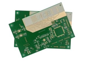
PCB and PCBA Must Work Together
High-quality electronic products require both a well-designed PCB and a well-controlled PCBA process.
A PCB with excellent electrical characteristics may still fail during assembly if its pads, component spacing, thermal relief, or solder-mask design are inappropriate.
Conversely, a highly capable PCBA Manufacturing process cannot compensate for fundamental problems in the PCB design.
This is why PCB design engineers and PCBA engineers should consider manufacturability and assembly requirements at an early stage.
Design for Manufacturing and Assembly
Design for Manufacturing (DFM) and Design for Assembly (DFA) are important bridges between PCB design and PCBA production.
During the design stage, engineers should evaluate:
- Minimum line width and spacing
- Pad dimensions
- Component clearance
- Solder-mask openings
- Via placement
- Fiducial marks
- Component orientation
- Panelization
- Assembly accessibility
- Test-point placement
Early DFM and DFA analysis can identify potential manufacturing and assembly problems before production begins.
This can reduce rework, shorten production cycles, and improve overall yield.
Quality Control in PCB and PCBA Production
Quality management is essential at both the PCB and PCBA stages.
For PCB fabrication, quality control may focus on:
- Material quality
- Layer registration
- Copper thickness
- Hole quality
- Etching accuracy
- Surface finish
- Impedance
- Electrical continuity
For PCBA production, quality control may focus on:
- Component verification
- Solder paste printing
- Placement accuracy
- Reflow profiles
- Solder-joint quality
- AOI results
- X-ray results
- Electrical testing
- Functional testing
A comprehensive quality system should also include process traceability and corrective-action procedures.
Kingda’s PCB and PCBA Capabilities
Kingda understands that reliable electronic products require close coordination between PCB Manufacturing and assembly processes.
For PCB projects, important factors such as board structure, materials, layer count, HDI requirements, impedance control, thermal performance, and manufacturing tolerances can be evaluated during the engineering stage.
For assembled products, SMT Assembly, component placement, soldering, inspection, and testing must be coordinated with the PCB design.
By considering fabrication and assembly requirements together, Kingda can help customers reduce manufacturing risks and improve product consistency.
Conclusion
When comparing PCB vs PCBA, there is no universal answer to which technology is more advanced.
PCB Design and PCB Manufacturing form the foundation of an electronic product, while PCBA Design, SMT Assembly, and PCBA Testing transform that foundation into a functional electronic assembly.
PCB technology is particularly demanding when products require high-speed signals, high density, advanced materials, HDI structures, and precise manufacturing.
PCBA technology becomes increasingly challenging when products involve fine-pitch components, complex packages, demanding soldering processes, automated inspection, and comprehensive functional testing.
Ultimately, successful electronic manufacturing depends on the combination of high-quality PCB engineering and reliable PCBA processes. By integrating design, manufacturing, assembly, testing, and quality control, manufacturers such as Kingda can help customers achieve better performance, higher production yield, and more reliable electronic products.