As electronic products continue to become smaller, lighter, and more integrated, manufacturers require highly efficient and reliable PCB Assembly technologies. Two of the most widely used technologies are Surface Mount Technology (SMT) and Through-Hole Assembly, commonly known as DIP Assembly.
Although SMT Assembly has become the dominant technology for modern electronic manufacturing, DIP Assembly remains essential for components that require mechanical strength, high power handling, or through-hole connections. Together, these processes form an important part of modern PCBA manufacturing.
Kingda provides integrated PCB and PCBA manufacturing services, including SMT Assembly, DIP Assembly, PCB fabrication, component assembly, inspection, testing, and quality control.
What Is SMT?
Surface Mount Technology (SMT) is an electronic assembly technology in which electronic components are mounted directly onto the surface of a printed circuit board rather than inserted through drilled holes.
Most SMT components have no leads or very short leads. Components are positioned on solder paste-coated pads and then permanently attached through a reflow soldering process. SMT has become one of the most widely adopted technologies in the electronics manufacturing industry because it supports high component density, automated production, and compact product designs.
A typical SMT Assembly process includes:
- Solder paste printing
- Solder paste inspection (SPI)
- Component placement
- Reflow soldering
- Automated optical inspection (AOI)
- Electrical testing
- Final inspection
Compared with traditional through-hole assembly, SMT allows more components to be placed in a smaller area and is particularly suitable for high-density electronic products.
Key Requirements for SMT Substrates
The PCB substrate is an important foundation for reliable Surface Mount Technology. A substrate must provide electrical interconnection while also supporting mechanical stability and thermal management.
A suitable PCB substrate should have the following characteristics:
- Sufficient dimensional stability
- Good surface flatness
- Appropriate thermal resistance
- Reliable dielectric properties
- Good mechanical strength
- Compatibility with soldering temperatures
- Suitable characteristics for rework
- Reliable adhesion between copper and dielectric materials
For conventional rigid PCBs, epoxy-based laminates such as FR-4 are widely used because they provide a good balance of electrical performance, mechanical strength, thermal resistance, flame retardancy, and cost.
The substrate also plays several important roles in an electronic assembly. It provides electrical connections, supports components mechanically, distributes power, provides signal paths, and helps dissipate heat.
Rigid PCB and Flexible PCB Substrates
PCB substrates can generally be divided into rigid and flexible types.
Rigid PCBs are widely used in computers, industrial equipment, communication systems, automotive electronics, consumer electronics, and many other applications. Common rigid PCB materials include FR-4 and other high-performance laminates designed for high-frequency, high-speed, thermal, or reliability requirements.
Flexible PCBs, or FPCs, are manufactured using thin and flexible dielectric materials, commonly polyimide. They are designed for applications where space is limited or where the circuit must bend, fold, or move during operation.
Flexible PCBs offer several advantages:
- Excellent flexibility
- Reduced assembly space
- Lightweight construction
- Ability to bend or fold
- Good suitability for dynamic applications
- Excellent performance in compact electronic products
However, flexible PCB assembly can be more challenging than rigid PCB assembly. Handling, positioning, support, soldering, and component placement require appropriate manufacturing controls, particularly for fine-pitch components.
PCB: The Foundation of Electronic Products
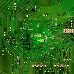
A PCB is one of the most important components in an electronic product. It provides the conductive patterns required to electrically connect electronic components according to a predetermined circuit design.
In simple terms, a PCB serves as both the electrical interconnection platform and the mechanical support structure for electronic components.
Modern PCBs are available in many configurations, including:
- Single-sided PCBs
- Double-sided PCBs
- Multilayer PCBs
- HDI PCBs
- Rigid PCBs
- Flexible PCBs
- Rigid-flex PCBs
- High-frequency PCBs
A typical rigid PCB consists of a dielectric substrate and copper foil. Depending on the board structure, copper layers may be present on one or both sides of the substrate or embedded within a multilayer stack-up.
Single-Sided PCB
A single-sided PCB contains conductive copper circuitry primarily on one side of the substrate. It is commonly used in relatively simple and cost-sensitive electronic products.
Double-Sided PCB
A double-sided PCB contains copper circuitry on both sides of the substrate. Plated through-holes are commonly used to establish electrical connections between the two copper layers.
Multilayer PCB
A multilayer PCB consists of multiple conductive layers separated by insulating dielectric materials. The layers are laminated together into a single structure, while vias provide electrical connections between different layers.
Multilayer construction enables designers to achieve higher circuit density and more sophisticated power and signal distribution within a limited board area.
From PCB to PCBA
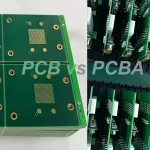
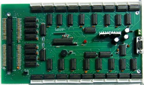
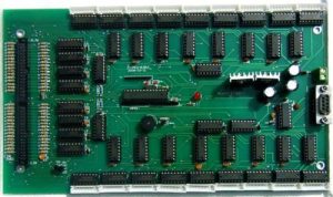
A bare PCB becomes a PCBA after electronic components have been mounted and soldered onto the board.
Therefore:
PCB = Bare printed circuit board
PCBA = Printed circuit board with electronic components assembled
A typical PCB Assembly process may combine SMT Assembly and DIP Assembly, depending on the component types and product requirements.
For example, small passive components and fine-pitch ICs are normally assembled using SMT, while connectors, transformers, large capacitors, switches, and other mechanically demanding components may use through-hole technology.
Complete PCBA Manufacturing Process
Modern PCB Manufacturing and assembly involve multiple controlled processes.
A typical PCBA production workflow includes:
- PCB fabrication
- Incoming material inspection
- Solder paste printing
- SPI inspection
- SMT component placement
- Reflow soldering
- AOI inspection
- DIP component insertion
- Wave soldering or selective soldering
- Manual soldering when required
- Cleaning
- Electrical testing
- Functional testing
- Final inspection
- Packaging and shipment
The exact process depends on PCB structure, component types, assembly density, product specifications, and reliability requirements.
Why PCB Cleaning Is Important
As electronic products become smaller, the distance between component leads, pads, and conductive structures continues to decrease. This trend increases the importance of PCB cleaning.
Historically, some manufacturers considered flux residues harmless because many flux materials are not highly conductive under normal conditions. However, modern high-density assemblies have much smaller clearances, making contamination more difficult to control.
Flux residues, ionic contamination, dust, and other process residues may contribute to:
- Electrical leakage
- Electrochemical migration
- Corrosion
- Insulation degradation
- Intermittent failures
- Long-term reliability problems
Therefore, cleaning requirements should be evaluated according to the flux chemistry, component density, product environment, reliability requirements, and applicable industry standards.
Kingda can incorporate appropriate inspection and process controls to help ensure that assembled boards meet the required cleanliness and reliability specifications.
What Is DIP Assembly?
DIP Assembly refers to the assembly of components using a dual in-line or other through-hole package configuration. DIP is one of the traditional through-hole packaging technologies and was widely used for integrated circuits before SMT became dominant.
DIP components typically have two parallel rows of leads that are inserted into corresponding holes in the PCB and then soldered.
Although many high-density products now rely heavily on SMT, through-hole technology remains valuable for components requiring strong mechanical connections or specific electrical and thermal characteristics.
Typical through-hole components include:
- Connectors
- Large transformers
- Relays
- Switches
- Power components
- Large capacitors
- Mechanical components
- Components subject to significant mechanical stress
DIP Assembly Process
DIP Assembly can involve both automated insertion and manual insertion.
A typical process includes:
- Component preparation
- Component identification
- Through-hole insertion
- Lead forming or trimming when necessary
- Component inspection
- Wave soldering or selective soldering
- Manual soldering for special components
- Post-solder inspection
- Electrical testing
- Final inspection
During manual insertion, operators must verify component reference designators, orientation, polarity, part numbers, and insertion positions.
Incorrect insertion or missing components can directly affect the electrical and functional performance of the final PCBA.
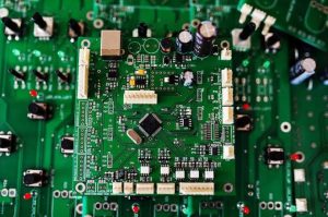
Wave Soldering and Selective Soldering
After through-hole components are inserted, wave soldering is commonly used for boards containing a large number of compatible through-hole components.
However, not every component can safely pass through a conventional wave soldering process. Certain components may be sensitive to heat, have special mechanical structures, or be located in areas unsuitable for wave soldering.
In such cases, manufacturers may use:
- Selective soldering
- Manual soldering
- Specialized soldering processes
The choice depends on component design, PCB layout, soldering requirements, thermal limitations, and production volume.
SMT vs. DIP Assembly
Both SMT and DIP have specific advantages.
| Feature | SMT Assembly | DIP Assembly |
|---|---|---|
| Component mounting | Surface mounted | Through-hole |
| Component density | Very high | Generally lower |
| Automation | Highly suitable | Suitable for many applications |
| Board space | Efficient | Requires additional through-hole area |
| Mechanical strength | Good | Excellent for many components |
| Fine-pitch capability | Excellent | Limited |
| Typical applications | ICs, resistors, capacitors, compact modules | Connectors, switches, power and mechanical components |
In many modern products, the best manufacturing strategy is not to choose between SMT and DIP, but to combine them according to the requirements of the product.
Quality Control in PCB Assembly
Reliable PCB Assembly requires multiple levels of quality control rather than relying on a single inspection method.
Kingda can use automated equipment together with manual inspection to establish multiple quality checkpoints throughout production.
Common inspection technologies include:
SPI
Solder Paste Inspection checks solder paste volume, height, area, position, and other parameters before component placement.
AOI
Automated Optical Inspection identifies problems such as missing components, incorrect placement, polarity errors, solder defects, and component-related abnormalities.
X-Ray Inspection
X-ray inspection is particularly useful for hidden solder joints, bottom-terminated components, BGAs, and other structures that cannot be fully inspected using conventional optical inspection.
Electrical Testing
Electrical testing can verify continuity, isolation, shorts, opens, and other electrical characteristics according to the product requirements.
Functional Testing
Functional testing evaluates whether the assembled PCBA performs its intended electrical or system-level functions.
Combining automated inspection, process monitoring, and manual verification provides stronger control than relying on a single inspection method.
Why Choose an Integrated PCB and PCBA Manufacturing Partner?
Managing PCB fabrication, component sourcing, SMT, DIP, inspection, testing, and final assembly through an integrated manufacturing partner can simplify production management and improve process traceability.
An experienced manufacturer should be able to coordinate:
- PCB fabrication
- Component procurement
- SMT Assembly
- DIP Assembly
- Soldering
- AOI and SPI inspection
- X-ray inspection
- Electrical testing
- Functional testing
- Rework and repair
- Final quality inspection
This integrated approach can help reduce communication gaps between different suppliers and provide better control over quality, delivery, and production consistency.
Kingda PCB and PCBA Manufacturing Services
Kingda provides integrated PCB and PCBA manufacturing solutions covering the complete production chain from bare PCB fabrication to assembled and tested electronic products.
Our capabilities can support different PCB structures, component packages, assembly requirements, and production volumes. By combining automated manufacturing equipment, process control, inspection systems, and experienced personnel, Kingda focuses on delivering stable and reliable electronic assemblies.
Whether a product requires high-density SMT, traditional through-hole components, mixed-technology assembly, flexible PCB assembly, or comprehensive testing, selecting the appropriate manufacturing process is essential to achieving reliable product performance.
As electronic products continue to move toward miniaturization, higher integration, higher speed, and greater functional complexity, the combination of PCB Manufacturing, SMT Assembly, and DIP Assembly will remain an important foundation of modern electronics manufacturing.