PCB Warpage: Causes, Hazards, and How to Prevent It
PCB warpage is the bending or twisting of a printed circuit board away from a flat plane. It usually shows up as bow, a cylindrical curve along the length or width of the panel, or twist, a diagonal deformation in which opposite corners no longer lie in the same plane. Even a deviation of a fraction of a percent of the board dimension is enough to confuse the vision systems and nozzles of a modern assembly line. As components get smaller and multilayer boards thinner and larger, flatness has become a fundamental reliability requirement.
A warped board rarely fails in an obvious way during inspection, but the damage appears downstream: components are placed out of position, fine-pitch leads lift from their pads after reflow, connectors no longer align with their housings, and finished assemblies cannot be seated in their enclosures. Placement machines, automated inspection systems and reflow conveyors all assume that the board surface is exactly where the process data says it is. Flatness must therefore be managed from base material pressing to final assembly.
The causes of board deformation are complex and interactive. Some stress enters while the copper clad laminate is pressed; more is added during multilayer lamination; solder mask curing and hot air solder leveling repeatedly heat and cool the panel; and storage, handling, material behavior and the copper layout of the original design all leave their mark. This article explains where the deformation comes from, what a warped board can do during PCB assembly, and how gopcb prevents PCB board deformation from reaching the field.

Why Flatness Matters: Hazards of Warped Boards in Assembly
The first casualty of board deformation is placement accuracy. When the panel is not flat, the board surface is higher or lower than the reference plane taught in the machine program, so components land out of position, fine-pitch leads miss their solder paste, and in severe cases a part simply cannot be seated on its pad at all. Automatic through-hole insertion equipment suffers too: a board lifted higher than expected can jam or damage the tooling.
The problems continue after soldering. If the board moves while the solder is molten, leads are dragged out of their joints or components stand up on one end, leaving weak or open connections. Once the assembly cools into a bow, depaneling is difficult because a curved panel cannot be cut cleanly, and the finished product may not fit into the housing, connector or socket for which it was designed. Warpage is one of the most common reasons a good design still fails in production, which is why contract manufacturers check incoming flatness on every SMT PCB assembly order.
The industry puts concrete numbers on these requirements. IPC criteria allow a maximum bow and twist of 0.75 percent of the board dimension for boards carrying surface mount components, and 1.5 percent for boards without them. Many manufacturers that depend on high-precision, high-speed SMT are stricter still, specifying 0.5 percent or even 0.3 percent so that vision systems always see a predictable surface.
Warpage That Starts in Copper Clad Laminate Production
The first source of stress lies inside the copper clad laminate itself. A standard double-sided laminate has a symmetrical structure and normally no copper pattern yet, and the expansion coefficients of copper foil and glass cloth are close, so mismatched expansion is rarely the direct cause of warpage. The danger is more subtle: press hot plates are never perfectly uniform in temperature, so the resin in different areas of the sheet cures at slightly different speeds and to slightly different degrees.
Different heating rates also change the dynamic viscosity of the resin during pressing, and uneven curing leaves local stress frozen into the sheet. While the laminate stays in one piece this stress is largely balanced and may never be noticed, but it does not disappear: when the material becomes a printed circuit board and is heated again, the trapped stress gradually releases and distorts it. Small curing variations in the very first pressing can therefore surface much later as measurable PCB board deformation.
Residual Stress Built Up During Multilayer Lamination
Multilayer lamination generates the most thermal stress in the whole PCB manufacturing flow. The bonding step resembles the pressing of copper clad laminate, but the conditions are much harder to control: the stack is thicker, the inner layer patterns are diverse, and several partially cured prepreg sheets must flow, bond and cure at the same time. Wherever curing proceeds faster or slower than the surrounding area, local stress is created, far harder to remove from a thick multilayer stack than from a simple laminate.
The trapped stress does not stay inside the panel forever. It releases gradually during later steps such as drilling, profile routing and baking, and each release deforms the board a little more. Because stress history builds up layer by layer, flatness depends on process discipline: stable press profiles, correct prepreg storage, controlled cooling and careful baking all reduce the residual stress that later steps set free. Flatness control therefore begins with consistent PCB manufacturing processes rather than with a measurement at the end of the line.
Warpage from Solder Mask and Legend Curing
Solder mask and legend baking are easy to underestimate because their temperatures seem mild, yet they are classic sources of board deformation. Solder mask inks cannot be stacked while they cure, so boards stand vertically in racks during baking. At about 150 degrees Celsius, curing sits at or above the glass transition temperature of many medium and low Tg laminates.
Above Tg, the resin turns soft and elastic and its stiffness drops sharply. A panel hanging vertically then becomes sensitive to its own weight and oven airflow, slowly creeping into a bow that becomes permanent when the material cools below Tg. Thin panels and low Tg materials are most vulnerable, so flatness-critical jobs need baking programs matched to the laminate Tg.
Thermal Shock in Hot Air Solder Leveling
Hot air solder leveling (HASL) is one of the most aggressive thermal processes that a bare board experiences. In a typical leveling line the solder bath runs at about 225 to 265 degrees Celsius, the board stays in the bath for only three to six seconds, and the hot air knives that strip excess solder operate at roughly 280 to 300 degrees Celsius. The board enters from room temperature and is cleaned and cooled back down within about two minutes of leaving the bath. The whole operation is a sudden heating and cooling cycle with almost no time for even heat distribution.
The internal structure of the board is not uniform: copper areas, resin-rich regions and glass cloth conduct heat at different rates and expand by different amounts, so thermal stress builds during every heating and cooling step. Part is released as micro strain, and strain that cannot relax symmetrically leaves the panel with a visible bow or twist. Boards carrying large ground planes are especially sensitive, because the copper heats quickly while the opposite side is still cool. For flatness-critical designs, many manufacturers now avoid HASL and select immersion finishes that impose less thermal shock.
Storage and Handling: Quiet Sources of Warpage
Even a perfectly flat board can be deformed between process steps, before a single component is placed. Bare boards usually wait vertically on racks or in stacks, and if rack tightness is set incorrectly or a stack is clamped unevenly, thin boards take on a permanent set. Boards thinner than 2.0 mm are most at risk: their low stiffness lets gravity and clamping pressure push the material past its elastic limit over time.
Handling discipline prevents most of this damage. Boards should be stored vertically with even support, spaced evenly in racks, and moved in batches small enough to avoid bending under their own weight. Delivery packaging matters too: cushioning between panels and support across the full area prevent the first bend of a new order in transit. These rules look simple, but they separate factories that deliver flat boards from factories that only measure the problem.
Design and Material Factors That Control Board Flatness
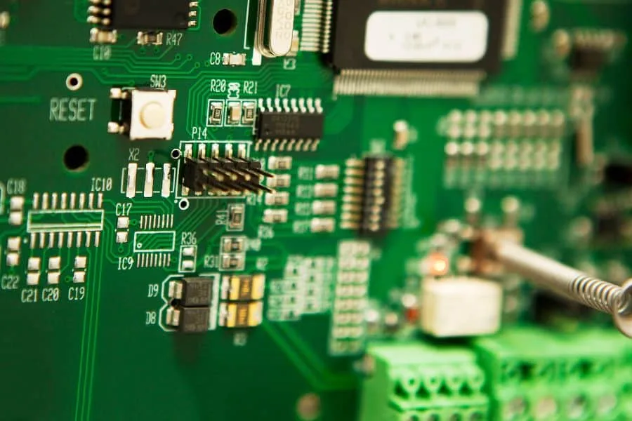
A printed circuit board is a composite of copper foil, resin and glass cloth, and each material has its own physical and chemical properties. Because the materials expand and contract at different rates whenever the board is heated, thermal stress is always present after pressing, and the stack geometry decides how that stress is released. A multilayer board that is not symmetrical through its thickness, with different layer counts or copper weights on the two halves, bends on cooling because the two sides shrink by different amounts.
The copper distribution on each layer matters just as much as the stackup. Ground and power planes often cover nearly a whole layer, and when such large copper areas sit unevenly on the same board, heat absorption and expansion differ across regions and the differential stress warps the panel. Near the upper limit of the glass transition range the resin softens, making deformation even easier.
The vias that connect the layers also influence the result. Through holes, blind vias and buried vias mechanically connect the layers and restrict free expansion and contraction. Under repeated thermal cycling, restricted expansion can release itself as twist, which is why a board may sit flat when new and warp only after years of service. Designers therefore control flatness from the start: symmetrical stackups, balanced copper on every layer, grid copper where full coverage is unnecessary, and Tg matched to the thermal processes the board must survive. These decisions are all made during PCB design layout, where they cost nothing, and are almost impossible to correct once fabrication begins.
How gopcb Controls Flatness in Production
gopcb treats board flatness as a process property rather than an inspection lottery. Press profiles are matched to each stackup, prepreg and laminate are stored under controlled conditions, baking programs account for material Tg, and thin boards are supported in fixtures while curing and cooling. Every panel is measured against IPC bow and twist criteria after profiling, flatness is verified again before the first print of solder paste, and results are logged per batch under the quality management system so drift is caught while still cheap to correct.
For customers who want the whole chain handled by one supplier, board fabrication and component assembly can be combined in a single turnkey PCB assembly service, so design files, materials, process records and quality data stay under one roof. Send gopcb your Gerber files, bill of materials and expected volumes for a free design for manufacturability review, and the engineering team will check the stackup, copper balance and flatness requirements before recommending the most cost-effective process for your product.