SMT Component Polarity: How to Identify Polarized Parts for PCB Assembly
Why Component Polarity Matters in SMT Assembly
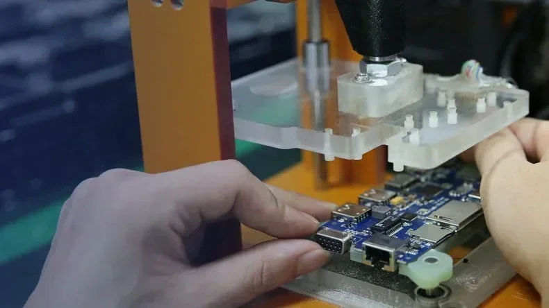
Surface mount technology places hundreds of small components on a printed circuit board in seconds, but a component is not installed correctly just because it lands in the right position; it must also face the right direction. Common SMT components include chip resistors, chip capacitors, inductors, diodes, transistors, integrated circuits, and fuses, and a large share of them are polarized, which means they only work when their positive and negative terminals, or their first pin, match the pattern printed on the board.
The difficulty is that most automated checks cannot see orientation before soldering. A reversed resistor or ceramic capacitor behaves like a correctly mounted one, so polarity only matters for a minority of parts, but that minority includes almost every active device and many power components. Diodes, LEDs, tantalum capacitors, aluminum electrolytic capacitors, and nearly all integrated circuits carry a clear orientation requirement, and one reversed part can turn an entire batch into rework or scrap. That is why orientation is treated as a process discipline on every SMT PCB assembly line rather than as an operator habit.
What a Polarity Defect Actually Means
Polarity means that the positive and negative terminals, or the first pin, of a component must point in the same direction as the positive and negative terminals, or the first pin, marked on the PCB. Board designers print the reference on the silkscreen layer, usually a plus sign, a band, a dot, or a chamfered corner, so the assembler can compare every part against a fixed pattern. When the direction of the component does not match the direction shown on the board, the result is called a reverse defect.
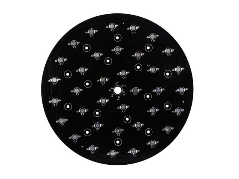
Some circuits tolerate a mistake better than others. A reversed diode may simply block the current and stop the board from working, while a reversed aluminum electrolytic capacitor can overheat, bulge, or vent, and a reversed tantalum capacitor may fail violently. An LED mounted backwards never lights, and an integrated circuit powered through reversed supply pins can be destroyed in milliseconds. Reverse defects are easy to create, easy to miss in a fast visual check, and hard to repair after soldering, so every polarized part should be verified before placement.
Polarity Marks on Capacitors and Inductors
Capacitors are divided into two large groups during SMT processing, and the two groups are handled very differently. Multilayer ceramic chip capacitors have no polarity and can be mounted in either direction. Tantalum capacitors, however, are always polarized: the anode end of a molded tantalum chip is marked with a colored band or a plus sign on the body, and the corresponding pad on the PCB carries the same indication. Inspection confirms that the marked end of the part lines up with the marked end of the footprint, because the two marks together define the only correct orientation.
Aluminum electrolytic capacitors are polarized as well, and they carry several marks that work together. The cylindrical body usually shows a stripe with minus signs on the negative side, and radial through-hole versions make the positive lead longer than the negative lead. On the PCB the positive pad is often marked with a plus sign, while the negative pad may be shaded, hatched, or drawn with a different outline. Cylindrical SMD types use a similar convention: the blackened segment printed on top of the can marks the negative terminal. These conventions are created during design and transferred to the board during PCB manufacturing, so a footprint with unclear marks should be checked against the component datasheet before placement.
Inductors follow a simpler rule. Chip inductors, wire-wound two-terminal coils, and ferrite beads have no polarity requirement and may be mounted in either direction. Multi-pin inductors, common-mode chokes, and transformer-style components are different, because their internal windings are not symmetrical. The manufacturer marks one terminal with a dot, a circle, or a printed number, and the corresponding pad on the PCB repeats the same reference, so the operator aligns the two marks exactly as with an integrated circuit.
Finding the Cathode on LEDs and Diodes
Light-emitting diodes are among the most common polarized components on modern boards. On a chip LED, the cathode side is identified by a small colored dot or a printed line on the body, and on many standard parts that dot is green. The PCB repeats the reference with a vertical bar, a color band, or a silkscreen mark at the cathode pad, and many footprints add an acute-angle corner or a box outline pointing to the same terminal. For through-hole LEDs, the cathode lead is shorter than the anode lead, and the rim of the package has a flat spot on the cathode side.
Diodes have two terminals and are polarized at both ends. On a surface-mount diode, the cathode is the end marked with a color band or stripe, and the PCB uses the same language: a vertical stripe, a color band, or an acute-angle triangle whose bar points to the cathode pad. Glass-body diodes carry a color ring at the cathode end, and some small-signal types use a groove or a colored mark. When the marks cannot be matched with confidence, the part should be checked against its datasheet, because a reversed diode can short a supply rail or silently disable the circuit around it.
Reading Pin One Marks on IC Packages and BGAs
Integrated circuits always carry an orientation reference, because their pins are connected to specific internal functions. On small-outline packages such as SOP and SOIC, pin 1 is marked with a dot, a notch, a molded dimple, or a ribbon or stripe near the first pin. Quad flat packages use a chamfered corner at the pin 1 position and often repeat the reference with a printed symbol on top of the body. Small transistor packages use the same idea, with a dot, a notch, or a differently shaped corner marking the reference pin. Some packages identify pin 1 by making one lead visibly different in size or shape, so the operator must inspect the part itself instead of relying only on the reel label.
Ball grid array packages deserve special attention, because the balls disappear under the component after placement and a rotation error can pass several intermediate checks. The BGA body carries a molded dimple, groove, dot, or circle at the A1 corner, and the PCB repeats the reference with a circle, a dot, the letter 1 or A, or a beveled corner. The polarity point of the part must correspond to the polarity point on the board, so the placement program is verified before the first board is soldered, and X-ray inspection confirms ball alignment after reflow.
Resistor Color Codes and Capacitor Value Codes
Orientation is not the only marking skill used on an assembly line; engineers and inspectors must also read the codes that define component values. The classic example is the axial resistor, whose color rings encode resistance and tolerance. The scale contains twelve standard colors: black, brown, red, orange, yellow, green, blue, violet, gray, white, gold, and silver. The first ten colors represent the digits zero through nine, while gold and silver are never digits; they represent tolerance values of plus or minus 5 percent and plus or minus 10 percent respectively.
A normal four-band resistor carries two digit rings, one multiplier ring, and one tolerance ring. The first two colors give the significant digits, so orange and black together represent the number 30. The third ring tells the reader how many zeros to add: if the third ring is red, two zeros are added and the value becomes 3,000 ohms, or 3 kΩ. If the fourth ring is silver, the finished part may measure anywhere within plus or minus 10 percent of 3,000 ohms, and if it is gold, the allowed window narrows to plus or minus 5 percent.
Capacitor markings follow a different logic. Electrolytic capacitors are printed directly with their capacitance value, working voltage, and polarity, so the information can be read straight from the cylindrical body. Small chip capacitors are marked with a three-digit code in which the first two digits are the significant figures and the third digit is the number of zeros that follow, with the value expressed in picofarads. For example, the code 233 means 23 followed by three zeros, or 23,000 pF, which equals 23 nF, or 0.023 µF. A code ending in zero, such as 470, is read directly: it means 47 pF, because no zeros are added.
How Assembly Lines Catch Orientation Errors Before Reflow
Most polarity defects are created before the component reaches the solder joint, so professional lines verify orientation at several moments. First, the engineering team reviews the bill of materials and the footprint library, making sure every polarized part has a correct pad pattern and a clear silkscreen mark. Second, the placement program is validated, because a component rotated 180 degrees inside the program will be placed backwards on every board of the batch. Finally, the first article of each new product is inspected before the line ramps up.
After reflow, automated optical inspection compares every polarized component with the expected orientation and flags any part whose mark does not match the footprint. AOI checks every board with consistent criteria across all shifts, which makes it well suited to polarity work. For hidden joints under BGAs and similar packages, X-ray inspection verifies that the balls are aligned with their pads, and in-circuit testing confirms that the circuit behaves correctly; the complete sequence is documented at the PCBA testing stage, and results are attached to the order.
Inspection results should feed back into the process instead of ending with a rejected board. If the same polarity error appears twice, the line engineer reviews the silkscreen mark, the feeder setup, the program rotation, and the training records, then records the corrective action so the root cause cannot repeat on the next batch.
How gopcb Handles Polarity-Sensitive Assembly
gopcb applies the same discipline to every order that enters its workshop. When the design files arrive, the engineering team reviews the bill of materials and the footprint library, confirms that every polarized component has a visible polarity mark, and flags unclear marks for correction at the design review. Feeders are loaded from verified lists, and each placement program is checked against the polarity references on the board. Customers who want one supplier for the whole job can place it through the gopcb PCB assembly service and keep every process record in one place.
Prototype boards are the cheapest place to find orientation problems, so gopcb recommends a small pilot run for every new design that contains BGAs, fine-pitch connectors, or dense arrays of polarized capacitors. Every production board is checked with automated optical inspection, and the results are logged against the order. Send gopcb your Gerber files, bill of materials, and expected volumes for a free DFM and manufacturability review, or combine fabrication and assembly under turnkey PCB assembly so design files, components, and quality records stay with a single accountable supplier.