PCBA Board Debugging Steps: A Practical Bring-Up Guide
Why PCBA Debugging Needs a Structured Routine
Bringing a newly designed PCBA sample to life is rarely as simple as loading the files, soldering the parts, and pressing the power button. When the board is large and carries hundreds of electronic components, the first power-on can expose reversed polarized parts, marginal solder joints, wrong resistor values, and control signals that never appear, and staring at the schematic rarely reveals which of them is the real problem. Engineers who master a reasonable set of debugging methods can reach ideal results much faster, because every PCBA board debugging step narrows the fault range before the next step begins.
The routine described here suits any board that has never been powered: a new prototype, a design revision, a reworked unit, or a first article from a production line. Each situation carries its own risks, yet the same logic applies. Checks that do not require power come first, components are added in stages instead of all at once, power is applied through a current-limited supply, and only then does the work move to voltage measurements and signal tracing. Working from the least risky procedure to the most invasive one protects the components and keeps the fault range small at every stage.
Debugging also produces knowledge worth keeping. The measurements and observations taken during bring-up often become the reference data used later in production testing, and faults found on the bench usually point to improvements in the design or the assembly instructions. With that in mind, here are the PCBA board debugging steps that experienced technicians follow when they meet a new sample for the first time.
Start With Visual Inspection and Rail Resistance Checks
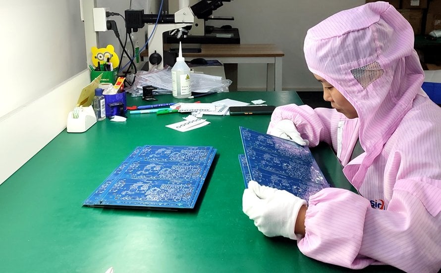
The first PCBA board debugging step costs nothing but time: look carefully at the board before anything is powered. The bare board should be checked for cracks, scratches, damaged solder mask, and lifted pads, while an assembled sample should be scanned for solder bridges, dry joints, tombstoned chips, shifted or missing components, reversed polarity, and solder balls left between pads. Components can also be damaged mechanically during SMT placement or handling, so look for cracked bodies, blackened surfaces, and deformed leads, and correct any defect before power is applied.
Next, use a multimeter to measure the resistance between the power and ground nets. Place one probe on a main supply rail and the other on ground, and repeat the measurement for every rail the design uses. A very low reading or a direct short warns of a solder bridge, a reversed component, or a damaged device, and it is far cheaper to find such problems with an ohmmeter than after power is switched on. Remember that some rails are low impedance by design because of large decoupling capacitors, so when in doubt, compare the reading with a known-good board before condemning a section.
Install Components in Stages, Not All at Once
A full board with every component fitted is hard to debug, because a fault in one module can hide behind the behavior of another. For this reason, experienced technicians install components and independent modules step by step rather than mounting everything at once. When each functional block is added separately, the fault range shrinks to the most recently installed parts: a problem that appears after a module is added almost certainly belongs to that module or its connections, so bring-up of a large board never has to feel overwhelming.
A practical order is to start with the power section, then add the clock and controller, then memory, and finally the interface and peripheral circuits. Powering the board after each stage instead of only at the end is the point of the exercise. When the power block runs cleanly on its own, later stages can be verified against a stable reference, and the same circuit blocks usually prove themselves again when the product moves to volume SMT PCB assembly.
Power On Safely With a Current-Limited Supply
Once the power components are in place, the next PCBA board debugging step is a controlled power-on. Attach the power module to the board and check that each output voltage is correct, but never apply full power to an unknown board from a fixed bench supply. Use an adjustable regulated power supply with a current limiting function, preset the overcurrent protection below the expected consumption, and then slowly raise the voltage while watching the input current, input voltage, and output voltage. If the current stays within the limit and the outputs reach their nominal values, the power section is healthy.
If the overcurrent protection trips, the voltage refuses to rise, or the current climbs far beyond the estimate from the bill of materials, switch the supply off immediately and search for the fault. A shorted rail, a reversed polarized capacitor, a wrongly placed regulator, or a solder bridge are all common causes. Correct the fault and repeat the same procedure until the power stage starts cleanly, because every later PCBA debugging step depends on stable rails.
Test Each Module as It Is Installed
With the power section verified, install the other modules one by one and power test each of them as it is added. After switching the supply on, repeat the overcurrent-safe routine and check the rails, the current draw, and the behavior of the newly fitted circuits. Testing each installed module in turn prevents the overcurrent and component burning that design errors or component installation errors could otherwise cause, because a mistake is detected while only a small part of the board is active.
Keep a simple log of what was measured at every stage: rail voltages, input current, temperatures, and anything unusual such as a faint whistle or a warm part that should stay cool. The log turns debugging from a memory exercise into a record that can be reviewed, and it becomes the starting point for the documented test procedure that production uses later, so boards brought up this way move smoothly from engineering into production testing and functional verification.
Use Voltage Measurement to Isolate Faults
Once the whole board is powered, the voltage measurement method is usually the first fault-finding tool. Confirm that the power pin of every chip on the PCB receives its correct supply voltage, then check the reference voltages called out on the schematic and the working voltage at each important node, because discrepancies identify the section to investigate. For example, when an ordinary silicon transistor is powered and conducting, its base-emitter junction voltage is about 0.7 V and its collector-emitter saturation voltage is about 0.3 V or less; if the base-emitter voltage is clearly higher than 0.7 V, except with special devices such as Darlington pairs, the junction is likely open.
On digital boards the same idea extends beyond supply pins. Verify the reset line, the clock, and the enable signals at each stage, and use an oscilloscope to check ripple and dynamic voltage drop under load instead of trusting a static multimeter reading alone. Moving through the schematic in signal order and comparing each measurement with the expected value quickly separates power problems from logic problems and shows where to concentrate.
Trace Faults With Signal Injection
The signal injection method finds faults in amplifier and processing chains. A known signal is applied to the input terminal, and the waveform is then measured stage by stage to find the point where the signal disappears, distorts, or changes amplitude incorrectly. In audio, video, and other amplification circuits a simple variant works without any generator: touch the input terminals of successive stages with tweezers and watch whether the output reacts. If touching the first stage produces no response but touching the second stage does, the fault lies in the earlier stage or its coupling, and the inspection should focus there.
One warning applies to every variant of this method. Signal injection must never be used on circuits with a hot backplane or on high-voltage sections, because touching live points can cause electric shock. Use proper probes, keep instrument grounds isolated where required, and follow ESD-safe handling so that the measurement itself does not damage the board under test.
Look, Listen, Smell, and Touch
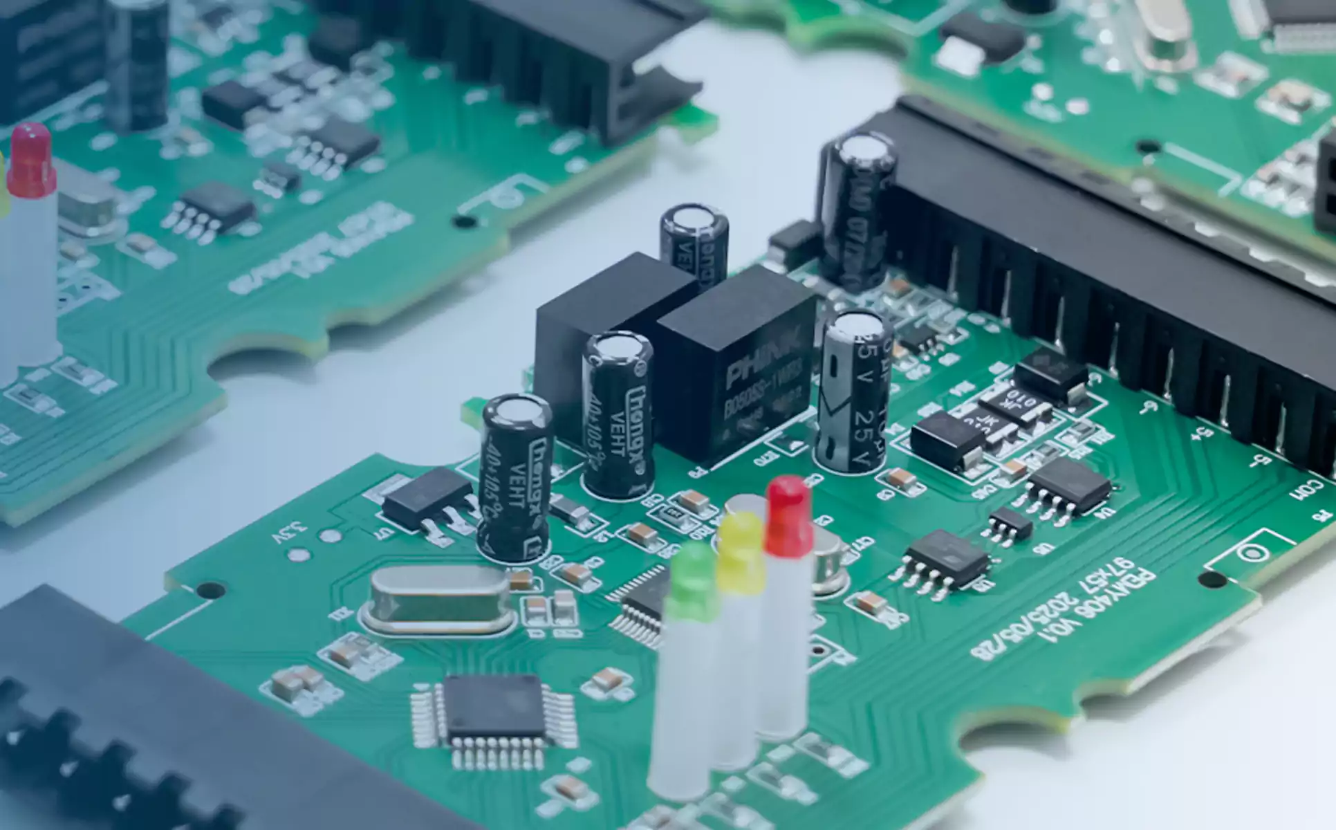
The senses offer fast clues that instruments sometimes miss, and experienced PCBA technicians use them throughout the debugging process. Looking means checking whether components were damaged mechanically by SMT equipment or handling: cracked bodies, blackened surfaces, deformed leads, and dull joints all tell a story. Listening means comparing the sound of the working board with what it should sound like; a converter that whistles, a relay that chatters, or an arc that hisses is a fault. Smelling is equally direct: the sharp odor of a burning PCB or the smell of leaking capacitor electrolyte means power down immediately and trace the hot part.
Touching is used to judge temperature while the board works, because electrical equipment produces heat when it operates. A power transistor or voltage regulator that is warm is normal, but a component that should be passing current yet feels cold is probably not working, and a part that should stay cool but cannot be held is oscillating, overloaded, or shorted. As a rough reference, a component that can be held for more than about three seconds is near 70 degrees Celsius, which is acceptable for general-purpose power transistors and regulators; if it cannot be held at all, investigate before continuing. For accurate readings use a thermocouple or thermal camera, and always be careful around live circuitry.
None of these checks replaces the electrical measurements from the earlier steps; they complement them. A warm regulator may simply be heavily loaded, and an odd smell can come from flux residue rather than a real fault, so confirm every observation with a multimeter or oscilloscope before replacing parts. Change one thing at a time, retest after each change, and record the result, because most debugging mistakes come from testing several hypotheses at once.
How gopcb Supports Clean Board Bring-Up
gopcb applies exactly this discipline when customer designs arrive for assembly. New and revised boards can be handled as prototype PCB assembly jobs, where the engineering team checks the files, assembles the sample under controlled conditions, and brings it up with current-limited power and staged module tests before any volume run starts. Visual inspection, electrical checks, and functional verification are documented for every build, so the debugging history of the board is available when production begins.
Many bring-up problems can also be prevented earlier. When the PCB design layout includes test points, clearly marked rails, and probe-friendly spacing, debugging time falls sharply, and the gopcb DFM review checks these details before fabrication. After assembly, every board is verified through PCBA testing with automated optical inspection and electrical tests, and customers who want the whole chain handled by one supplier can combine fabrication, component sourcing, and assembly under turnkey PCB assembly. Send gopcb your Gerber files, bill of materials, and expected volumes for a free DFM and manufacturability review, and the team will recommend the best bring-up and test strategy for your product.