PTFE PCB and Ceramic PCB: Choosing by Dk, Loss and Heat
Two substrate families dominate the top of the circuit board market, and they are chosen for different reasons. A PTFE board is chosen for its electrical behaviour: a low dielectric constant, a very low loss and a stable response over frequency. A ceramic board is chosen for its thermal behaviour: high thermal conductivity, a coefficient of thermal expansion close to that of the components mounted on it and mechanical stiffness.
Because the two are often quoted as alternatives, the comparison is frequently made on the wrong axis. A design does not choose between them on cost alone; it chooses on whether the limiting factor is signal integrity, heat or dimensional stability, and the answer is usually visible in the first page of the requirements.
What Each Substrate Is
A PTFE board is built on a polytetrafluoroethylene matrix, usually reinforced with glass or filled with a ceramic powder to control its expansion and its mechanical properties. The pure material is soft and difficult to process, so the filled and reinforced grades are what a fabricator will normally quote.
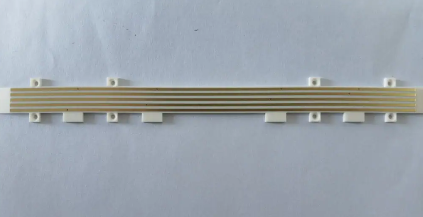
A ceramic board is usually an alumina substrate, either as a sintered plate used with thick film or thin film metallisation, or as a ceramic filled organic laminate that behaves like a very stiff, thermally conductive PCB. The two are often grouped together, although their fabrication routes have little in common.
Electrical Performance and Loss
The dielectric constant of an unfilled PTFE material is close to 2.2, and its dissipation factor can be below 0.001 across a wide band. That combination keeps the traces wide for a given impedance and keeps the loss low, which is why the material appears in microwave and millimetre wave designs.
Alumina has a dielectric constant around 9 to 10, so a microstrip on ceramic is much narrower for the same impedance. Its loss is low but higher than that of a good PTFE grade, and its dielectric constant varies more with frequency. Where the design is loss limited, PTFE wins; where the design is size limited, ceramic does.
Thermal Conductivity and Power Handling
Alumina conducts heat at a rate that an organic laminate cannot approach, which allows a power device to be mounted directly on the substrate and to dissipate through it. This is the reason ceramic appears in power amplifiers, in LED modules that run hot and in high frequency circuits where the device and the matching network share one substrate.
A PTFE board removes heat through copper and through thermal vias, so the thermal path is a design task rather than a property of the material. Where the power density is moderate that is entirely practical, and the metal backed variants of the material allow a heat spreader to be bonded underneath the circuit.
Dimensional Stability and Expansion
Ceramic is stiff and its expansion coefficient is low, close to that of silicon, so a bare die mounted on ceramic sees far less stress during thermal cycling than the same die on an organic substrate. That matching is the main reason ceramic is used for large area devices and for applications with a demanding cycle life.
PTFE is softer and expands more, although the filled grades are much better than the base material. Where a large device has to be attached over a long span, the expansion mismatch becomes a design constraint and the answer may be a stiffener, a smaller die or a different substrate rather than a different adhesive.
Fabrication and Process Differences
PTFE processing requires attention to drilling, because the material is soft and tends to smear rather than cut cleanly, and to plating, because the surface needs an activation step before copper will adhere. Panel shrinkage and the dimensional behaviour during lamination also differ from FR4, which changes how the artwork is compensated.
Ceramic substrates are processed differently again. Thick film circuits are printed and fired, thin film circuits are deposited and etched in a clean environment, and the ceramic filled laminates are processed more like a conventional board. None of those routes tolerate the same design rules, so the choice of substrate is also a choice of supply chain and of the fabricator who can build it.
Cost, Size and Application Fit
The material cost of a PTFE board is higher than FR4 and lower than a ceramic substrate of the same area, but the comparison is misleading without the processing cost. A thick film ceramic circuit avoids the drilling, the plating and the multilayer lamination altogether, so for a simple high frequency circuit it can be competitive even at a higher material price.
Size follows from the dielectric constant. A ceramic circuit can be far smaller for the same electrical function, which matters when the module has to fit inside a package, while a PTFE circuit will be larger but easier to integrate with a conventional assembly process.
Design Checklist
Decide which parameter is limiting before choosing a material. If the budget is set by insertion loss, start from the PTFE family and confirm that the fabricator can hold the impedance; if it is set by junction temperature or by thermal cycling of a large die, start from ceramic and confirm the metallisation and the attachment process.
Then check the mechanical interface: the stiffener, the housing, the connector and the way the module is mounted all change the stress that reaches the substrate. gopcb supports high frequency laminates, metal backed constructions and ceramic filled materials, and can advise which of them meets a given loss or thermal target without an unnecessary cost premium.
Specifying the Substrate on a Drawing
The fabrication drawing for a PTFE PCB has to state more than a material name. It should give the grade or at least the dielectric constant and the loss target, the copper weight and the surface finish, the dielectric thickness between the layers that carry controlled impedance traces and the tolerance on that thickness. Without those numbers the fabricator will choose a stackup that meets the outline, and the electrical performance measured on the first article will be a surprise rather than a confirmation.
A ceramic PCB drawing is different in the same way that the process is different. The metallisation thickness, the conductor adhesion and the firing temperature define what the circuit can carry, and the attachment method for the devices is part of the substrate specification rather than a separate assembly note. Whether the ceramic is a sintered plate with fired conductors or a ceramic filled laminate determines which of those numbers applies, so the first line of the specification has to say which construction is intended.
FAQ
Is PTFE always lower loss than ceramic? For a given geometry, the unfilled PTFE grades have the lowest dissipation factor, but the filled grades and the circuit geometry both matter, so the comparison should be made on the actual stackup.
Can a ceramic substrate be used for a large board? It can, but the size is limited by the firing process and by the cost of the substrate. Large circuits are usually split into modules and mounted on a carrier.
Which material is better for a high power RF amplifier? Ceramic, normally, because the heat leaves through the substrate. Where the power is moderate, a PTFE board with thermal vias and a bonded heat spreader can meet the same target at lower cost.
Related reading: high frequency trace routing, high temperature PCB materials, microstrip and stripline routing, and PCB manufacturing tolerances.