Radar PCB Design: Materials, Phase Matching and Thermal Path
A radar board is a mixed-signal assembly at the extreme end of the spectrum. It carries microwave transmit and receive paths, high-speed digital processing, and a power stage, often on a single multilayer stack inside a sealed module.
The design problem is not any one of those domains but the interaction between them. The transmit pulse disturbs the receive chain, the digital processing injects noise into the analog front end, and the thermal load from the power amplifier shifts the electrical length of the feed network.
What the Board Has to Support
The board carries the antenna feed network, the transmit and receive switching, the low-noise receive path, the data conversion and the processing interface. In an active array, it also distributes power and control to many identical channels.
In a phased array, the channel-to-channel consistency matters more than the absolute performance of any single channel. Amplitude and phase must match across channels, which turns the layout into a tolerance and symmetry problem.
Material Selection
Radar frequencies make dielectric loss a first-order concern, so low-loss laminate is used on the RF layers. The dielectric constant must be stable across frequency and temperature, because the electrical length of the feed network changes with it.
Hybrid stackups are standard: low-loss material for the RF layers and standard FR-4 for the digital and power layers. That keeps cost proportionate while preserving the electrical performance where it matters.
Where a very stable material is needed, a ceramic-filled PTFE laminate with a tightly specified dielectric constant is used, and the design geometry is calculated from that value rather than from an FR-4 rule of thumb.
Phase Stability and Channel Matching
Phase stability is the property that keeps the beam pointing where it should. It depends on the physical length of each path, the dielectric constant and its variation with temperature, and the consistency of the transitions in each channel.
Layout rules follow: keep the feed network symmetric, match path lengths to a small fraction of a wavelength, use identical transitions for every channel, and route the RF lines over a continuous reference plane.
Even the launch into each channel should be geometrically identical. A phase difference introduced by a connector transition cannot be corrected by the phase shifter without consuming range, and it varies with temperature in a way that is difficult to calibrate out.
Mixed-Signal Grounding
Radar boards combine microwave, analog and high-speed digital circuits. The ground strategy must define the return path for each of them, then join the regions at points that are controlled rather than incidental.
The microwave section needs a continuous reference plane with dense stitching vias, the analog section needs a quiet reference, and the digital section produces broadband noise. Connecting them at a single point near the data converter, and keeping the return currents separated elsewhere, is the standard approach.
Plane splits should be used sparingly. A split in a reference plane under an RF line creates a discontinuity, and the resulting reflection is often worse than the noise the split was intended to isolate.
Thermal Management
The power amplifier is the dominant heat source, and its junction temperature determines both reliability and output stability. Thermal vias under the device, copper planes that spread heat, and a path into the module housing are the standard measures.
Temperature also affects electrical performance. A feed network that changes electrical length with temperature will shift the beam, so the thermal design and the RF design are coupled. Where the shift matters, materials with a low temperature coefficient are chosen for the critical lines.
Power Distribution
An active array delivers power to many channels, each drawing a modest current but with fast switching transients during a transmit pulse. The power network must supply those pulses without sagging, which requires local energy storage at each channel.
Distribution is usually done in plane layers with dense via arrays, and the decoupling capacitors are placed as close to the amplifiers as the layout allows. The impedance of the vertical path through the board is often the limiting factor.
Assembly and Test
Radar assemblies frequently use metal-backed boards, connectors with controlled impedance and sometimes wire-bonded or flip-chip devices. Each of those adds assembly steps and inspection requirements.
Test covers each channel’s gain and phase, the isolation between transmit and receive paths, and the noise figure of the receive chain. Because channel matching is critical, test data is recorded per channel rather than as a single pass or fail.
Where the assembly includes a radome or a waveguide transition, the mechanical alignment becomes part of the electrical performance, and the board outline and mounting features carry tolerances that a standard board would not.
Design Checklist
Confirm the material and dielectric tolerances against the required phase stability, verify the symmetry of the feed network, check the reference plane continuity under every RF line, size the thermal path from the power amplifier to the housing, and confirm the power distribution can supply the transmit pulse.
Then review the mechanical interface: connector positions, waveguide alignment and the flatness of any surface that mates with a heat spreader. On a radar module, mechanical and electrical performance are the same problem.
Related reading: microwave PCB materials and fabrication, high-frequency data bus routing, and mixed-signal PCB design guidelines.
Material and Layer Choices
A radar PCB usually moves onto a low-loss laminate for the RF layers while keeping a conventional FR-4 grade for the digital and power sections of the same stack. Mixing material classes inside one board is normal, but the transitions between them have to be planned rather than discovered during fabrication. The dielectric constant and the loss tangent of the RF laminate decide the trace width for a target impedance and the attenuation at the operating frequency, so both values belong in the stackup drawing rather than in a note on the side.
Layer count follows the number of distinct reference planes the design needs. Each RF signal layer wants an undisturbed ground plane underneath, the digital section wants its own ground and power pair, and the power stage wants copper thick enough to carry the transmit current without a large temperature rise. On a radar PCB, eight to twelve layers is common, and the copper weight on the outer layers is often raised to two ounces so that the transmit pulse does not produce a measurable voltage drop across the feed network.
Routing Discipline
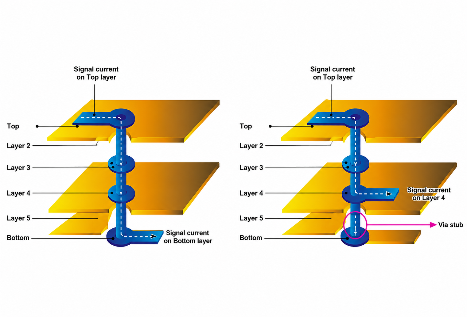
Every microwave trace is a transmission line, so the routing is designed as a continuous controlled-impedance path from the switch to the antenna port. Bends are mitred or replaced by swept curves, stubs are avoided, and vias are either removed from the RF path or compensated with a modelled transition. Where a via is unavoidable, the ground return vias are placed close to the signal via so that the return current has a short path and the discontinuity stays small.
On a radar PCB the isolation between the transmit and receive paths is a layout property as much as a circuit property. Physical separation, ground-via fences between the two chains and a continuous reference plane under the receive line all reduce leakage that would otherwise raise the noise floor and mask weak returns.
FAQ
Why is phase matching so important in a radar board? Because the beam direction is set by the relative phase of the channels. A mismatch steers the beam away from its intended direction and reduces the array gain.
Can FR-4 be used in a radar design? Only for the digital and power layers. The RF layers require a low-loss material with a stable dielectric constant, otherwise loss and phase drift degrade the performance.
What limits channel-to-channel consistency? Physical path length, dielectric variation and transitions. All three should be made identical by design rather than corrected in calibration.