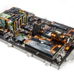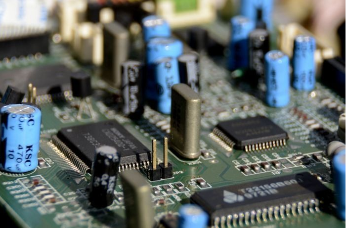
When designing a Multilayer PCB for a server, gaming platform, industrial controller, or other complex electronic system, designers often divide the system into several rigid circuit boards and install them inside a common enclosure.
However, a conventional rigid PCB is not always the best solution when the mechanical structure requires tight bends, unusual geometries, or three-dimensional interconnections. Flexible circuits can solve these problems, but using separate flexible cables or flexible PCBs may increase assembly complexity and cost.
What if the advantages of rigid and flexible circuits could be combined into a single PCB structure?
This is where a Rigid-Flex PCB becomes an effective solution.
By integrating rigid PCB sections with flexible circuit sections, rigid-flex technology can simplify system interconnections, save valuable enclosure space, reduce the number of connectors and cables, and improve electrical and mechanical reliability.
What Is a Rigid-Flex PCB?
A Rigid-Flex PCB is a circuit board that combines rigid PCB sections with one or more flexible circuit sections in a single integrated structure.
In a conventional Multilayer PCB design, different functional circuits may be distributed across multiple rigid boards. These boards then need to be connected using board-to-board connectors, cables, or other interconnection methods.
Although connectors can provide reliable electrical connections, they require additional space and components. Cables can provide greater mechanical flexibility, but they may create routing challenges, increase assembly steps, and occupy valuable space inside compact enclosures.
A rigid-flex structure integrates the interconnection directly into the PCB.
In simple terms, two or more rigid PCB sections are electrically connected by a flexible circuit section. The flexible portion acts as an integrated interconnect that can bend or fold according to the mechanical requirements of the product.
This makes rigid-flex technology particularly suitable for compact products with complex three-dimensional structures.
Why Use Rigid-Flex PCB Technology?
The main advantage of a Rigid-Flex PCB is that it combines the mechanical strength and component-support capability of rigid PCBs with the flexibility and space-saving characteristics of flexible circuits.
Key benefits include:
- Reduced number of board-to-board connectors
- Reduced cable and wire harness requirements
- Lower assembly complexity
- Better use of limited enclosure space
- Support for three-dimensional PCB configurations
- Improved mechanical integration
- Fewer electrical interconnection points
- Potentially improved signal integrity
- Improved resistance to vibration when properly designed
- Greater freedom in product mechanical design
For compact electronic products, reducing the number of connectors and cables can also simplify assembly and reduce potential points of electrical or mechanical failure.
Basic Structure of a Flexible Circuit
A typical Flexible Circuit consists of several fundamental materials.
The flexible section may include:
- Flexible polyimide substrate
- Copper conductor layer
- Adhesive layer
- Coverlay
Polyimide is commonly used because it provides good flexibility, thermal stability, dimensional stability, and electrical insulation.
The copper layer provides the conductive paths required for power and signal transmission.
In adhesive-based constructions, an adhesive layer bonds the copper to the flexible substrate. In other constructions, adhesiveless flexible materials may be used to achieve improved dimensional stability or thinner structures.
The coverlay protects the flexible copper circuitry from mechanical damage, contamination, and environmental exposure.
Depending on the application, a flexible circuit may contain multiple copper layers, allowing more complex routing and electrical functionality.
How the Rigid and Flexible Sections Are Combined
The rigid portion of a Rigid-Flex PCB is typically constructed using conventional PCB materials and multilayer manufacturing techniques.
Common materials and structures include:
- FR-4 or other rigid dielectric materials
- Prepreg bonding materials
- Copper foil
- Solder mask
- Surface finish
- Silkscreen or component identification markings
During fabrication, the flexible section and rigid section are laminated into an integrated PCB structure.
The rigid areas provide mechanical support for components, connectors, and other hardware, while the flexible areas provide controlled bending and three-dimensional routing.
Depending on the stackup and manufacturing process, the flexible layers may extend continuously through the rigid and flexible regions, while rigid dielectric materials are selectively added to create the rigid sections.
This structure allows designers to create a PCB that can be folded into the required mechanical configuration without relying on separate cables.
Rigid-Flex PCB as a Folded Circuit
From a system-design perspective, a Rigid-Flex Design can be viewed as a folded PCB.
Instead of manufacturing several independent rigid boards and connecting them with cables or connectors, the rigid sections can be positioned at different angles and connected through integrated flexible sections.
This can significantly reduce the number of interconnection points within the system.
For example, a rigid-flex board can connect:
- Main processing circuitry
- Power-management circuitry
- Display modules
- Sensors
- Cameras
- Communication modules
- Battery or power sections
The flexible section can be bent during final assembly to follow the internal geometry of the enclosure.
As a result, rigid-flex technology can help designers make better use of three-dimensional space.

Common Rigid-Flex PCB Stackup Configurations
There are several possible PCB Stackup configurations for rigid-flex designs. The appropriate structure depends on electrical performance, mechanical requirements, layer count, impedance requirements, manufacturing capabilities, and reliability targets.
Symmetrical Stackup
In a symmetrical configuration, the flexible layers are positioned near the center of the overall stackup.
A balanced construction can help reduce mechanical stress and warpage during lamination.
This configuration is often considered when electrical and mechanical requirements can be satisfied with a balanced layer arrangement.
Odd-Layer Stackup
Although even layer counts are common in conventional multilayer PCB structures, an odd number of layers may sometimes be used when required by electrical or mechanical constraints.
An additional copper layer may provide shielding or reference-plane functionality in the flexible region.
For high-speed applications, the stackup must be evaluated carefully to ensure that impedance, return-current paths, and electromagnetic compatibility requirements are satisfied.
Asymmetrical Stackup
If the flexible layers are not located near the center of the stackup, the structure may become asymmetrical.
An asymmetrical design can sometimes be useful when different areas of the PCB have significantly different dielectric thickness, impedance, routing, or via requirements.
However, asymmetry can increase the risk of mechanical deformation, warpage, and bending stress.
Therefore, appropriate lamination processes and mechanical tooling may be required during manufacturing.
Blind Vias and Buried Vias in Rigid-Flex PCB Design
Vias play an important role in multilayer rigid-flex structures.
A blind via connects an outer layer to one or more internal layers without passing through the entire PCB.
A buried via connects internal layers without being exposed on the outer surface.
In rigid-flex structures, via selection requires additional consideration because the flexible region must withstand repeated or controlled bending.
Complex via structures may therefore be concentrated in rigid sections whenever possible.
When vias must be used near flexible areas, designers should carefully consider via location, copper distribution, bend zones, pad geometry, and mechanical stress.
Avoiding unnecessary vias in dynamic bending areas can improve long-term reliability.
EMI Shielding for Flexible Sections
One of the important considerations in Rigid-Flex Design is electromagnetic interference (EMI) control.
Flexible circuits can act as transmission paths for high-speed signals, power, and sensitive analog signals. If the flexible section does not have an appropriate reference structure, it may become more susceptible to electromagnetic coupling and noise.
Depending on the application, shielding films or conductive shielding structures can be applied over the flexible section.
A shielding layer can be connected to an appropriate ground structure through conductive adhesive or other qualified interconnection methods.
This approach can provide electromagnetic shielding without significantly increasing the overall thickness of the flexible section.
For high-speed applications, however, shielding should not be treated as a substitute for proper stackup design. Signal-reference relationships, return-current paths, controlled impedance, trace spacing, and grounding must all be considered together.
High-Speed Signal Integrity in Rigid-Flex PCB Design
Rigid-flex technology is increasingly used in products containing high-speed interfaces and dense electronic systems.
However, simply integrating rigid and flexible circuits does not automatically guarantee good signal integrity.
Designers should consider:
- Controlled impedance
- Differential-pair routing
- Return-current paths
- Reference planes
- Trace geometry
- Dielectric thickness
- Crosstalk
- EMI
- Connector elimination
- Via transitions
The transition between rigid and flexible sections is particularly important.
Changes in dielectric thickness, copper geometry, reference planes, or trace structure can introduce impedance discontinuities.
Therefore, the electrical stackup should be designed as a complete system rather than treating the rigid and flexible portions as completely independent circuits.
Mechanical Design Considerations
The mechanical behavior of the flexible section is one of the most important aspects of Rigid-Flex PCB design.
Designers should define the bending requirements before completing the PCB layout.
Important factors include:
- Minimum bend radius
- Bend direction
- Number of bending cycles
- Static or dynamic bending
- Copper thickness
- Number of flexible layers
- Material selection
- Copper grain direction
- Component placement
- Via placement
- Stiffener requirements
Components should generally be kept away from areas intended for bending.
Vias, plated features, and other rigid structures should also be avoided in dynamic flex zones whenever possible.
For applications involving repeated bending, the flexible section must be designed according to the required bend radius and expected cycle life rather than simply the minimum physical space available.
Manufacturing Considerations for Rigid-Flex PCBs
A successful Rigid-Flex Design must consider manufacturing requirements from the beginning.
Rigid-flex fabrication is more complex than conventional rigid PCB manufacturing because the process must control both rigid and flexible materials.
Important manufacturing considerations include:
Material Compatibility
The rigid and flexible materials must be compatible during lamination and subsequent processing.
Differences in thermal expansion, dimensional stability, and mechanical properties can influence registration and reliability.
Layer Registration
Rigid-flex structures often contain complex layer transitions. Accurate registration is therefore essential for reliable drilling, routing, pad formation, and interconnection.
Flexible Area Protection
The flexible region must be protected from unnecessary mechanical damage during fabrication.
Material handling, routing, drilling, lamination, and assembly processes should all account for the characteristics of the flexible substrate.
Stiffeners
Polyimide or other stiffening materials may be added to selected flexible areas.
Stiffeners can improve mechanical support around connectors, component areas, or assembly interfaces while allowing other portions of the circuit to remain flexible.
Rigid-Flex PCB vs. Conventional PCB and Cable Assemblies
A conventional rigid PCB may be more economical for simple, flat electronic products.
Flexible PCBs are highly useful when bending and three-dimensional routing are required.
A rigid-flex structure becomes particularly attractive when both rigid component mounting and flexible interconnection are required within the same product.
Compared with a traditional rigid-board-and-cable assembly, rigid-flex technology can offer:
| Design Aspect | Conventional Rigid PCB + Cable | Rigid-Flex PCB |
|---|---|---|
| Interconnections | More connectors and cables | Integrated flexible interconnection |
| Assembly | More manual operations | Simplified assembly |
| Space utilization | Requires cable routing space | Better 3D space utilization |
| Mechanical integration | Limited | Excellent flexibility |
| Connector count | Usually higher | Can be reduced |
| Signal path | More interconnection transitions | More direct routing |
| Design complexity | Lower for simple products | Higher at PCB design/manufacturing stage |
| Initial PCB cost | Usually lower | Usually higher |
| System-level integration | Moderate | High |
Although rigid-flex PCBs may have higher fabrication costs than simple rigid boards, the overall system cost can be reduced when fewer connectors, cables, assembly operations, and mechanical parts are required.
When Should You Consider a Rigid-Flex PCB?
A Rigid-Flex PCB is worth considering when one or more of the following conditions apply:
- The product has a compact or irregular enclosure.
- Multiple rigid boards must be connected in a limited space.
- Cable assemblies are difficult to route.
- The product requires three-dimensional folding.
- Connector count needs to be reduced.
- Mechanical vibration is a concern.
- High-density interconnections are required.
- Signal integrity can benefit from shorter interconnection paths.
- The flexible circuit must be integrated directly into the PCB.
- Assembly space is limited.
For simple flat products, however, a conventional multilayer rigid PCB may remain the more economical solution.
Designing Rigid-Flex PCBs with Manufacturability in Mind
A strong PCB Design approach should consider electrical, mechanical, and manufacturing requirements simultaneously.
Before beginning the detailed layout, designers should define:
- The rigid and flexible regions.
- The required bend radius.
- The number of bending cycles.
- The layer count for each region.
- Controlled-impedance requirements.
- High-speed signal paths.
- Ground and reference structures.
- Via restrictions in flex areas.
- Stiffener locations.
- Component keep-out zones.
- Material and thickness requirements.
- Manufacturing tolerances.
Early collaboration between PCB designers, mechanical engineers, and the PCB manufacturer can significantly reduce redesigns.
For complex rigid-flex projects, 3D PCB design software is also valuable because it allows designers to verify the folded configuration and check mechanical interference before fabrication.
Kingda’s Approach to Rigid-Flex PCB Design
Kingda can support customers with PCB manufacturing solutions for applications requiring complex rigid and flexible structures.
For a Rigid-Flex Design, the manufacturing process should be considered together with PCB layout, material selection, stackup design, impedance requirements, mechanical bending, via structures, and assembly requirements.
By evaluating electrical and mechanical requirements at the beginning of the project, Kingda can help customers develop PCB solutions that balance performance, reliability, manufacturability, and overall system cost.
Conclusion
A Rigid-Flex PCB combines the structural advantages of rigid PCBs with the flexibility of flexible circuits. This makes it an effective solution for compact electronic products, high-density systems, and applications requiring complex three-dimensional mechanical configurations.
Compared with separate rigid boards connected by cables and connectors, rigid-flex technology can reduce interconnections, simplify assembly, improve space utilization, and potentially improve electrical and mechanical reliability.
However, rigid-flex technology also requires careful consideration of PCB Design, PCB Stackup, bend radius, via placement, material selection, impedance control, EMI performance, and manufacturing processes.
When electrical, mechanical, and manufacturing requirements are considered together from the beginning, rigid-flex technology can provide a highly integrated solution for modern electronic products.