Designing a Rigid-Flex PCB requires close coordination between PCB design and manufacturing. Unlike a conventional rigid or flexible circuit board, a rigid-flex board combines rigid and flexible sections within the same structure. Different regions may therefore require different materials, layer configurations, coverlay structures, and fabrication processes.
Understanding the manufacturing process is essential for creating accurate design data and avoiding unnecessary production issues. For designers working on rigid-flex or flexible circuit projects, manufacturing documentation is not simply a collection of output files. It is an important communication tool between the designer and PCB manufacturer.
At Kingda, early communication between design and manufacturing teams helps ensure that the proposed construction, materials, stackup, and fabrication methods are practical and manufacturable.
Why Fabrication Files Matter in Rigid-Flex PCB Design
Fabrication files communicate the designer’s manufacturing requirements to the PCB manufacturer. If these files are incomplete, ambiguous, or incorrectly structured, they can lead to misunderstandings, engineering changes, production delays, and additional costs.
For Rigid-Flex PCB Design, fabrication documentation is particularly important because the rigid and flexible sections may have different physical structures.
A complete manufacturing package should clearly define:
- Board outline and dimensions
- Rigid and flexible regions
- Layer configuration
- Material types
- Copper thickness
- Coverlay requirements
- Stiffener locations
- Cutout and routing requirements
- Drill information
- Plated and non-plated holes
- Surface finish
- Controlled impedance requirements
- Special manufacturing notes
The more complex the rigid-flex construction, the more important it is to provide clear and unambiguous manufacturing data.
Follow Appropriate Industry Standards
Designers should use recognized industry standards when preparing Fabrication Files for rigid-flex circuits. IPC standards provide commonly accepted terminology and design guidance that can help designers and manufacturers communicate more effectively.
For rigid-flex applications, IPC-2223 is an important reference for flexible and rigid-flex printed board design. The applicable revision and related standards should always be confirmed with the PCB manufacturer because manufacturing capabilities and project requirements may vary.
The key principle is simple: involve the PCB manufacturer early and make sure both sides use consistent terminology and documentation practices.
A manufacturer with experience in Rigid-Flex PCB fabrication can identify potential manufacturing risks before the design is released for production.
Gerber vs. ODB++ for Rigid-Flex PCB Manufacturing
Gerber remains a widely used format for PCB fabrication data. However, complex rigid-flex designs can benefit from a more structured intelligent manufacturing-data format.
ODB++ can provide a more comprehensive representation of PCB manufacturing information, including layer structures and design attributes. When supported by the manufacturer’s CAM system, it can reduce the amount of manual interpretation required during engineering review.
For complex Rigid-Flex PCB Design, designers should confirm which data format the manufacturer prefers before generating the final manufacturing package.
The important point is not simply choosing one file format over another. The manufacturer must be able to correctly interpret the supplied data and understand the intended rigid and flexible construction.
Clearly Define Rigid and Flexible Regions
One of the biggest challenges in Rigid-Flex PCB Design is clearly identifying where the rigid section ends and the flexible section begins.
A rigid-flex board may contain multiple structural regions, such as:
- Rigid PCB areas
- Flexible circuit areas
- Stiffened flexible areas
- Component-mounting regions
- Bend zones
- Transition regions
- Cutout areas
Each region may have different material and stackup requirements.
For example, a flexible region may use polyimide-based materials and coverlay, while a rigid section may use FR-4 or another rigid laminate. A stiffened flexible area may combine flexible materials with additional reinforcement.
These regions should be clearly identified in the manufacturing documentation.
Define the Stackup for Each Region
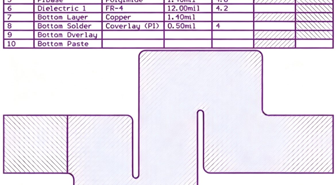
The PCB Stackup is one of the most important documents in a rigid-flex project.
Unlike a conventional multilayer PCB, a rigid-flex board can have different numbers of active layers and different materials in different physical regions. Therefore, a single simplified stackup drawing may not adequately describe the complete construction.
A practical approach is to use mechanical or documentation layers to define each region and associate the region with its corresponding stackup.
For example, the fabrication package can identify:
Region A — Rigid Section
FR-4-based multilayer construction with solder mask and standard PCB surface finish.
Region B — Flexible Section
Polyimide-based flexible construction with copper layers and coverlay.
Region C — Reinforced Flexible Section
Flexible construction combined with a stiffener to support component mounting or mechanical handling.
This regional approach gives the manufacturer a much clearer understanding of the intended construction.
Use Mechanical Layers to Define Construction Areas
Mechanical layers can be extremely useful when documenting a Rigid-Flex PCB.
Designers can duplicate or reference the board outline and clearly mark the boundaries of different structural regions. Each region can then be assigned an identifier corresponding to a detailed PCB Stackup table.
This documentation should clearly indicate:
- Where rigid material is present
- Where flexible material is exposed
- Where coverlay is required
- Where stiffeners are installed
- Where components may be mounted
- Where bending is permitted
- Where bending must be avoided
- Where mechanical cutouts are required
Clear graphical documentation can significantly reduce interpretation errors during CAM preparation and manufacturing.
Coverlay Requirements in Flexible Areas
Coverlay is an important part of Flexible PCB construction. It provides insulation and mechanical protection for exposed copper traces in flexible regions.
When designing a rigid-flex circuit, the coverlay should not be treated as an ordinary solder mask layer. Its opening dimensions, registration, material thickness, and bonding requirements should be considered separately.
The fabrication documentation should clearly define coverlay openings around:
- Solder pads
- Component mounting areas
- Contact areas
- Test points
- Required exposed copper regions
For component mounting on a flexible section, additional reinforcement may also be required to provide sufficient mechanical support.
Stiffeners and Reinforced Flexible Areas
Flexible circuits are designed to bend, but some areas must remain mechanically stable for component assembly or connector insertion.
Stiffeners are commonly used to reinforce selected areas of a flexible circuit. Depending on the design, materials such as FR-4, polyimide, or other suitable reinforcement materials may be used.
In a Rigid-Flex PCB, stiffeners should be clearly defined because they affect the local thickness, mechanical flexibility, and assembly characteristics of the board.
The designer should specify the stiffener location, material, thickness, and attachment requirements according to the application and manufacturer’s capabilities.
Drilling and Plated Through-Hole Considerations
Drilling requires particular attention in rigid-flex construction.
A hole passing through a rigid section and continuing into a flexible region may require a different manufacturing approach from a conventional rigid PCB. Certain holes may also need to be treated differently depending on whether they are plated, non-plated, or associated with a specific rigid-flex region.
The fabrication package should therefore clearly identify:
- Plated through holes
- Non-plated through holes
- Blind and buried vias where applicable
- Hole sizes and tolerances
- Drill depths
- Hole-to-edge requirements
- Flexible-region restrictions
Unnecessary or poorly planned holes can increase manufacturing complexity and reduce yield. Designers should therefore work with the manufacturer to determine the most practical via and drilling strategy.
Bend Areas and Bend Radius
Mechanical flexibility is one of the defining characteristics of a Flexible PCB and rigid-flex circuit.
The bend region should be clearly identified in the design documentation. Designers should avoid placing unnecessary vias, plated holes, large components, or other rigid structures in areas intended to bend.
The minimum bend radius depends on factors such as:
- Number of flexible layers
- Copper thickness
- Flexible material
- Coverlay structure
- Dynamic or static bending requirements
- Local stiffeners
- Application environment
For dynamic applications, the mechanical design requirements can be significantly more demanding than for a board that is bent only once during assembly.
Manufacturing Collaboration Is Essential
The most effective way to reduce rigid-flex manufacturing problems is to involve the manufacturer during the early design stage.
A PCB manufacturer experienced in Rigid-Flex PCB production can review the proposed structure and identify potential issues involving:
- Layer transitions
- Material selection
- Bend zones
- Copper distribution
- Via placement
- Coverlay openings
- Stiffener design
- Drill strategy
- Fabrication tolerances
- Assembly requirements
This early Design for Manufacturing (DFM) review can prevent problems that might otherwise be discovered only after the fabrication files have been released.
Kingda’s Approach to Rigid-Flex PCB Manufacturing
At Kingda, the manufacturing review of a Rigid-Flex PCB focuses on connecting design intent with practical production requirements.
During engineering review, the rigid and flexible regions can be evaluated separately to determine the appropriate material combinations, PCB Stackup, drilling structure, coverlay design, stiffener requirements, and fabrication tolerances.
Clear manufacturing documentation also helps Kingda’s engineering and production teams interpret the design consistently. For complex boards, structured manufacturing data such as ODB++, when supported by the customer’s design workflow and manufacturing system, can further improve data communication.
The goal is to ensure that the final manufacturing package accurately represents the intended board construction while minimizing ambiguity and unnecessary production risk.
Conclusion
A successful Rigid-Flex PCB Design requires more than creating the electrical schematic and PCB layout. Designers must clearly communicate the physical construction, material requirements, flexible regions, rigid regions, coverlay, stiffeners, drilling, and PCB Stackup to the manufacturer.
Accurate Fabrication Files are therefore essential to successful rigid-flex production. Standardized terminology, appropriate manufacturing-data formats such as ODB++, and early collaboration with an experienced PCB manufacturer can significantly reduce engineering misunderstandings and improve manufacturability.
As rigid-flex technology continues to support smaller, lighter, and more integrated electronic products, close cooperation between designers and manufacturers will remain essential. By combining detailed documentation, practical DFM review, and controlled manufacturing processes, Kingda supports reliable Rigid-Flex PCB solutions for demanding electronic applications.