

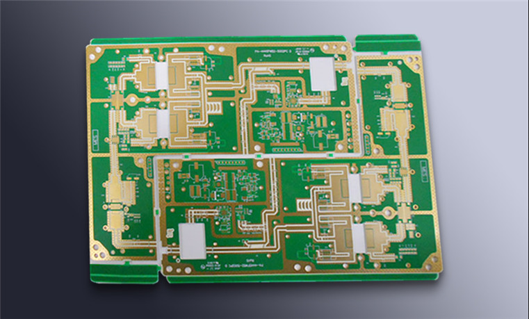
With the rapid development of the electronics industry, electronic products are becoming increasingly smaller, lighter, and more powerful. This trend has created both opportunities and challenges for PCB Manufacturing and electronic assembly technologies.

Modern electronic devices such as smartphones, communication equipment, automotive electronics, medical devices, industrial control systems, and wearable products require higher circuit density, improved reliability, and more precise manufacturing processes.

After a bare PCB completes the surface mounting process and undergoes the complete assembly procedure, the finished product is called a PCBA (Printed Circuit Board Assembly). PCBA Manufacturing integrates PCB production, component placement, soldering, inspection, and testing into a complete electronic assembly solution.

Traditional through-hole assembly methods can no longer meet the requirements of high-density electronic products. Therefore, SMT Assembly (Surface Mount Technology Assembly) has become the mainstream manufacturing method due to its advantages of high efficiency, high precision, and excellent electrical performance.

As a professional PCB and assembly manufacturer, Kingda provides comprehensive PCB Assembly solutions, combining advanced production equipment, strict quality management systems, and professional manufacturing experience to support customers with reliable electronic products.

What Is SMT Assembly?

Surface Mount Technology (SMT) is an advanced electronic assembly technology that directly mounts surface-mount components onto the surface of a PCB.

Compared with traditional through-hole assembly, SMT Assembly offers several advantages:

  • Higher component density
  • Smaller product size
  • Improved production efficiency
  • Better electrical performance
  • Reduced manufacturing costs
  • Suitable for automated production

The complete SMT process includes solder paste printing, component placement, reflow soldering, cleaning, inspection, testing, and packaging.

Each process step directly affects the final quality and reliability of the PCBA product.

1. SMT Programming and Component Placement Setup

Before production begins, engineers need to prepare the manufacturing program according to customer-provided design files, including:

  • BOM (Bill of Materials)
  • PCB layout files
  • Component coordinates
  • Assembly requirements

The placement program defines the exact position, angle, and mounting parameters of each component.

During this stage, engineers verify component specifications and optimize placement paths to ensure efficient and accurate production.

Kingda uses professional manufacturing systems to manage production data, reduce programming errors, and ensure consistency throughout the SMT Assembly process.
                                           

2. Solder Paste Printing

Solder paste printing is the first major step in PCB Assembly.

A stencil is placed above the PCB, and solder paste is accurately applied onto designated component pads through stencil openings.

The quality of solder paste printing directly affects solder joint reliability.

Important process parameters include:

  • Solder paste thickness
  • Printing pressure
  • Printing speed
  • Stencil accuracy
  • PCB positioning accuracy

Kingda uses advanced automatic solder paste printing equipment and high-quality solder materials to achieve stable printing performance and reduce defects such as:

  • Insufficient solder
  • Excess solder
  • Solder bridging
  • Misalignment

A precise printing process provides a strong foundation for subsequent component placement and soldering.

3. Component Placement

After solder paste printing, surface-mounted components are accurately placed onto the PCB pads using high-speed placement machines.

The placement process requires extremely high precision because modern electronic products often contain:

  • Micro components
  • Fine-pitch ICs
  • BGA packages
  • 0201 and smaller components

Advanced placement equipment can achieve micron-level accuracy, ensuring that each component is positioned correctly.

Kingda applies automated SMT Assembly equipment and strict process control to guarantee placement accuracy and production efficiency.

The main advantages include:

  • High-speed placement
  • High positioning accuracy
  • Stable production quality
  • Compatibility with various component types

4. Reflow Soldering

Reflow soldering is a critical stage in PCB Assembly.

During this process, the PCB passes through a reflow oven where temperature profiles are carefully controlled.

The solder paste melts at high temperatures and forms reliable solder joints between electronic components and PCB pads.

A typical reflow process includes:

  1. Preheating zone
  2. Thermal soaking zone
  3. Reflow zone
  4. Cooling zone

Proper temperature control is essential to avoid:

  • Cold solder joints
  • Component damage
  • Solder cracking
  • PCB deformation

Kingda uses advanced multi-zone reflow soldering systems to ensure uniform heating and stable solder quality for different PCB materials and component structures.

5. PCB Cleaning Process

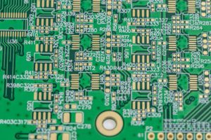
After Reflow Soldering, some flux residues and other contaminants may remain on the surface of the PCB. If these residues are not removed, they may affect electrical performance, reliability, and long-term product stability.

Therefore, PCB cleaning is an important step in the PCBA Manufacturing process.

The cleaning process mainly removes:

  • Flux residues
  • Dust particles
  • Oil contamination
  • Metal particles
  • Other manufacturing impurities

Depending on product requirements, manufacturers may use different cleaning methods, including:

  • Water-based cleaning
  • Semi-aqueous cleaning
  • Solvent cleaning
  • No-clean process

For high-reliability electronic products, such as automotive electronics, medical equipment, and industrial control systems, strict cleaning standards are required to ensure long-term operational stability.

Kingda applies appropriate cleaning processes according to customer requirements and product applications to maintain PCB surface cleanliness and improve product reliability.

6. PCB Inspection and Quality Control

Quality inspection is a critical stage in PCB Assembly. Through advanced inspection equipment and strict quality management, manufacturers can identify defects and ensure that every PCBA meets design requirements.

Common inspection methods include:

Automated Optical Inspection (AOI)

AOI Inspection uses high-resolution cameras and intelligent software algorithms to automatically detect PCB assembly defects.

It can identify problems such as:

  • Component missing
  • Incorrect component placement
  • Wrong component polarity
  • Solder bridging
  • Insufficient solder
  • Excess solder

Compared with manual inspection, AOI provides higher inspection speed and better consistency, making it an essential technology in modern SMT Assembly production.

X-Ray Inspection

For hidden solder joints such as BGA, QFN, and other advanced packages, traditional optical inspection cannot directly detect internal defects.

X-ray inspection technology can analyze internal solder connections and identify:

  • Voids
  • Poor solder joints
  • Insufficient solder filling
  • Hidden assembly defects

This technology is especially important for high-density and high-reliability PCB products.

Electrical Testing

Electrical testing verifies whether the assembled PCB functions according to the design requirements.

Common testing methods include:

  • In-circuit testing (ICT)
  • Functional testing (FCT)
  • Flying probe testing

These tests help detect:

  • Open circuits
  • Short circuits
  • Incorrect connections
  • Electrical performance issues

Kingda combines multiple inspection technologies to create a complete quality control system throughout the PCBA Manufacturing process.

7. Functional Testing and Final Verification

After assembly and inspection, finished PCB assemblies undergo final testing to confirm their electrical and functional performance.

Functional testing simulates real operating conditions to verify whether the product works correctly.

The testing process may include:

  • Power-on testing
  • Signal verification
  • Communication testing
  • Performance evaluation
  • Reliability checks

For customized electronic products, Kingda works closely with customers to develop suitable testing solutions based on application requirements.

This ensures that each PCB Assembly product delivered to customers meets performance expectations.

8. PCBA Packaging and Shipment

After passing all inspections and tests, qualified PCB assemblies enter the packaging stage.

Proper packaging protects PCBA products from:

  • Electrostatic discharge (ESD)
  • Mechanical damage
  • Moisture
  • Dust contamination

Common packaging materials include:

  • Anti-static bags
  • ESD foam
  • Protective trays
  • Customized packaging solutions

For components that are sensitive to impact or electrostatic damage, specialized packaging methods are used to ensure safe transportation.

Kingda follows strict packaging standards to protect product quality from production to delivery.

Kingda’s PCBA Manufacturing Advantages

As an experienced electronics manufacturing partner, Kingda provides integrated PCB Manufacturing and SMT Assembly services, supporting customers from prototype development to mass production.

Key advantages include:

Advanced Production Capability

Kingda applies automated manufacturing equipment and professional production management systems to ensure:

  • High production efficiency
  • Stable quality
  • Accurate component placement
  • Consistent assembly performance

Strict Quality Management

Quality control is implemented throughout the entire manufacturing process, including:

  • Incoming material inspection
  • PCB inspection
  • SMT process monitoring
  • Soldering quality control
  • Final product testing

Flexible Manufacturing Solutions

Kingda supports various PCB and assembly requirements, including:

  • Prototype production
  • Small-batch manufacturing
  • Medium-volume production
  • High-volume manufacturing

Solutions can be customized according to product complexity, application environment, and reliability requirements.

Conclusion

With the continuous development of electronic technology, modern products require smaller size, higher integration, and stronger reliability. SMT Assembly has become a key technology for achieving advanced electronic manufacturing.

A complete PCBA Manufacturing process includes solder paste printing, component placement, reflow soldering, cleaning, inspection, testing, and packaging. Every step directly affects the final quality and performance of electronic products.

Through advanced equipment, professional engineering support, and strict quality control, Kingda provides reliable PCB Assembly solutions for industries including communication, automotive electronics, industrial control, medical equipment, and consumer electronics.

As electronic products continue to evolve toward higher density and smarter functions, advanced PCB Manufacturing and SMT technologies will remain essential for future innovation.

Leave A Comment

