PCB Substrate Defects: Blowholes, Adhesion Loss, and Dimensional Drift
Most board defects are discussed in terms of copper, plating, or assembly, but a significant share originates in the base material itself. The laminate determines how the board expands with temperature, how strongly the copper adheres to it, and how much volatiles it releases during soldering. When one of those properties is out of specification, the symptom appears somewhere else entirely, which makes it easy to blame the wrong process. The PCB substrate defects below are the three most common failure families and what causes them.
The common thread is that each one is a material or process interaction that shows up under thermal load, so a board can pass every electrical test at room temperature and fail during assembly or after a few hundred thermal cycles.
Blowholes and Cold Solder Joints
A blowhole is a rupture in the solder joint or in the barrel wall caused by gas expanding inside the hole as the board is heated. The pattern is characteristic: a volcano-shaped opening, a joint with a visible void, or a pinhole in the plated wall. The defect appears after wave soldering or reflow, not before, which is why it is often attributed to the assembly process.
The actual mechanism usually begins during wet processing. Volatiles absorbed by the laminate are sealed in by the coating, and when the board is subsequently heated that trapped material expands and pushes out through the weakest point, which is the plated barrel or the joint itself. Laminate materials differ in how much moisture they absorb and how much they release, and poor plating quality makes the barrel more vulnerable to the pressure.

The countermeasures are material and process based. Reduce the moisture content of the panel before soldering by baking it according to the laminate manufacturer’s recommendation, improve the plating quality so the barrel can withstand the internal pressure, and select a material with lower Z-axis expansion when the thermal load is severe. The Z-axis expansion coefficient is the property that most directly predicts whether a barrel will survive the thermal excursion.
Adhesion Loss and Pad Separation
The second family of defects is the loss of the bond between the copper and the substrate. The symptom is a pad or a trace that lifts during soldering, during rework, or during a mechanical operation, and the failure is commonly described as poor adhesion strength or low peel strength.
Several mechanisms produce the same result. Excessive stress in the plated copper, introduced by aggressive plating chemistry or by an over-energetic etch, can lift a pad when the board is heated. Mechanical operations such as punching or routing can partially separate a pad without removing it, and the damage becomes evident only during hole metallization. Solder operations performed above the material’s rated temperature, or for longer than the profile allows, degrade the bond directly. Component weight and repeated rework add mechanical load to the same interface.
Where the separation occurs at the same location on every board, the cause is usually the layout rather than the process. A heavy copper area connected to a small pad, a wide trace meeting a pad at an abrupt angle, or a large thermal mass adjacent to a thin feature all create a local mismatch in thermal expansion, and the bond fails at that point repeatedly. The design answer is to balance the copper distribution and avoid abrupt transitions, which is the same principle that governs thermal relief design.
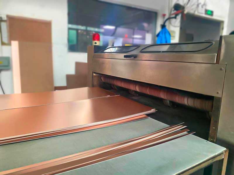
Diagnosing adhesion problems requires information the fabricator holds: the solvents and solutions used at each wet process step, the dwell times and temperatures, and the results of peel testing on incoming material. That data is worth requesting when a pad separation problem appears, because it narrows the cause to a specific operation instead of the whole flow.
Dimensional Variation After Processing
Boards that no longer fit the tooling or the enclosure after processing have a dimensional stability problem. The board may exceed its tolerance in one direction, fail to align with the fixture, or show a different shrinkage than the previous lot. Because the error appears after lamination, drilling, or soldering, the cause is often sought in those operations when the material is the real source.
Two mechanisms dominate. The first is the fiber orientation of the reinforcement. A woven glass fabric expands and shrinks differently along the warp and weft directions, and the difference can be substantial. If panels are cut without respecting a consistent orientation, boards produced from the same lot will change dimensions by different amounts, and the variation will not be reproducible. The second is residual stress locked into the laminate during manufacture. If that stress is not relieved, it releases during subsequent thermal processing and produces an irregular change in dimension.
The controls are straightforward once the cause is known. Specify and maintain a consistent grain direction for all panels, verify that incoming material is within its dimensional specification, and ask the laminate supplier how residual stress is managed before processing. Consistent orientation also improves mechanical behavior, since the stiffness of the board differs along the two axes.
Material Selection as Prevention
The choice of laminate determines how much margin the process has. Higher glass transition temperature raises the temperature at which the material softens and its expansion behavior changes, which protects the plated holes. Lower moisture absorption reduces the driving force behind blowholes. A lower Z-axis expansion coefficient reduces the strain that a barrel experiences during thermal cycling. Where a board will see wide temperature excursions, these three properties are more important than the dielectric constant.
Where copper must bond to a material with poor adhesion characteristics, the fabricator can apply a bonding treatment, but the treatment has to be specified and verified rather than assumed. Copper foil selection interacts with the same trade-off, since the low-profile foils that improve high-frequency loss also bond less aggressively. Related material and process questions are covered in copper plating defect prevention.
Detection Before It Reaches the Customer
Incoming inspection should verify material properties from the supplier’s certificate and, where the risk justifies it, from a coupon test rather than from a certificate alone. Thermal stress testing of a coupon, followed by a microsection of the plated holes, reveals both plating quality and the material’s response to heat.
Production monitoring should track the process parameters that affect these mechanisms: lamination cycle, plating chemistry, bake time before soldering, and soldering profile. When a defect appears, the question to ask first is what changed in those parameters, because the answer is usually more informative than the defect itself. Solder alloy and profile choices interact with the same thermal limits, as discussed in lead-free versus leaded solder, and long-term dimensional behavior is covered in PCB dimensional stability and expansion.
FAQ
Do blowholes always indicate a plating problem? No. They indicate that gas was generated and could not escape, which can come from absorbed moisture in the laminate, from trapped process chemistry, or from plating defects that weakened the barrel. The plating is one contributor among several, which is why the diagnosis requires both a microsection and a review of the wet-process history.
Why does the same pad lift on every board? Because the cause is geometric rather than random. A repeated failure at one location usually reflects a thermal expansion mismatch created by the local copper distribution, a heavy component, or a trace geometry that concentrates stress. Changing the layout at that point resolves it.
How much dimensional change is normal after processing? The laminate datasheet specifies the expected range, and the acceptance criterion is that the board meets its mechanical tolerance after all processing. Variation beyond the specified range indicates either an orientation problem in panel cutting or residual stress that was not relieved, and either condition should be raised with the material supplier rather than compensated for in the design.